
Data Sheet

15
PCA9546A
www.ti.com
SCPS148G –OCTOBER 2005–REVISED MAY 2016
Product Folder Links: PCA9546A
Submit Documentation FeedbackCopyright © 2005–2016, Texas Instruments Incorporated
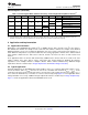
Control Register (continued)
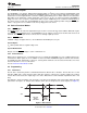
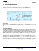
(1) Several channels can be enabled at the same time. For example, B3 =0, B2 = 1, B1 = 1, B0 = 0 means that channels 0 and 3 are
disabled, and channels 1 and 2 are enabled. Care must be taken not to exceed the maximum bus capacity.
Table 1. Control Register Write (Channel Selection), Control Register Read (Channel Status)
(1)
B7 B6 B5 B4 B3 B2 B1 B0 COMMAND
X X X X X X X
0 Channel 0 disabled
1 Channel 0 enabled
X X X X X X
0
X
Channel 1 disabled
1 Channel 1 enabled
X X X X X
0
X X
Channel 2 disabled
1 Channel 2 enabled
X X X X
0
X X X
Channel 3 disabled
1 Channel 3 enabled
0 0 0 0 0 0 0 0
No channel selected,
power-up/reset default state
9 Application and Implementation
9.1 Application Information
Applications of the PCA9546A will contain an I
2
C (or SMBus) master device and up to four I
2
C slave devices.
The downstream channels are ideally used to resolve I
2
C slave address conflicts. For example, if four identical
digital temperature sensors are needed in the application, one sensor can be connected at each channel: 0, 1, 2,
and 3. When the temperature at a specific location must be read, the appropriate channel can be enabled and all
other channels switched off, the data can be retrieved, and the I
2
C master can move on and read the next
channel.
In an application where the I
2
C bus will contain many additional slave devices that do not result in I
2
C slave
address conflicts, these slave devices can be connected to any desired channel to distribute the total bus
capacitance across multiple channels. If multiple switches will be enabled simultaneously, additional design
requirements must be considered (See Design Requirements and Detailed Design Procedure).
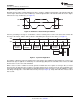
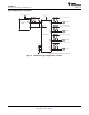
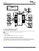
9.2 Typical Application
A typical application of the PCA9546A will contain anywhere from 1 to 5 separate data pull-up voltages, V
DPUX
,
one for the master device (V
DPUM
) and one for each of the selectable slave channels (V
DPU0
– V
DPU3
). In the
event where the master device and all slave devices operate at the same voltage, then the pass voltage, V
pass
=
V
DPUX
. Once the maximum V
pass
is known, V
CC
can be selected easily using Figure 12. In an application where
voltage translation is necessary, additional design requirements must be considered (See Design Requirements).
Figure 11 shows an application in which the PCA9546A can be used.