
Data Sheet

A
NA
S 1 1 1
0 A2 A1 A0
1
SDA
P
B3 B2 B1 B0
Start Condition R/W ACK From Slave NACK From Master Stop Condition
Slave Address Control Register
0 0 0 0
A AS 1 1 1 0 A2 A1 A0 0
Start Condition
SDA
R/W ACK From Slave ACK From Slave
P
B0B1B2B3XXXX
Stop Condition
Slave Address
Control Register
Data Output
by Transmitter
SCL From
Master
Start
Condition
S
1 2 8 9
Data Output
by Receiver
Clock Pulse for ACK
NACK
ACK
13
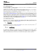
PCA9546A
www.ti.com
SCPS148G –OCTOBER 2005–REVISED MAY 2016
Product Folder Links: PCA9546A
Submit Documentation FeedbackCopyright © 2005–2016, Texas Instruments Incorporated
Programming (continued)
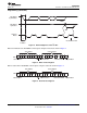
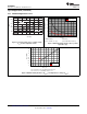
Figure 6. Acknowledgment on the I
2
C Bus
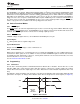
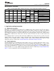
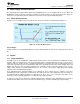
Data is transmitted to the PCA9546A control register using the write mode shown in Figure 7.
Figure 7. Write Control Register
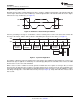
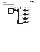
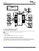
Data is read from the PCA9546A control register using the read mode shown in Figure 8.
Figure 8. Read Control Register