
User's Manual


Maps and Registers System Configuration Registers
114 SPARC/CPU−56T
System Configuration Registers
The CPU board implements a set of system configuration registers via the
field−programmable gate array (FPGA), which is accessible via the EBus.
The CPU Board System Configuration registers are used to control the on−board functions
and to receive status information of the board. It is subdivided into 16 areas with 16 Bytes,
each provided with a special function or reserved for future use.
a
In the following an overview of the System Configuration registers in the CPU board
address space is given. Every register is described separately in the following chapters.
Overview of System Configuration Registers
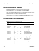
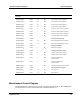
The table below shows an overview of all registers in the CPU board address space.
Table 25: CPU Board System Configuration Register Address Map
Address Range in
PA<40:0>
Size Access Default Description
1FF.F160.0100
16
16 Byte aa aa Function Unit Miscellaneous Control
1FF.F160.0100
16
1 Byte r/w 00
16
Miscellaneous Control register
1FF.F160.0110
16
16 Byte aa aa Function Unit Display
1FF.F160.0110
16
1 Byte r/w 00
16
LED 1 Control register
1FF.F160.0111
16
1 Byte r/w 00
16
LED 2 Control register
1FF.F160.0112
16
1 Byte r/w 00
16
LED 3 Control register
1FF.F160.0113
16
1 Byte r/w 00
16
LED 4 Control register
1FF.F160.0120
16
16 Byte aa aa Function Unit External Failure
1FF.F160.0120
16
1 Byte r 00
16
External Failure Status register
1FF.F160.0130
16
16 Byte aa aa Function Unit Watchdog
1FF.F160.0130
16
1 Byte r/w 08
16
Watchdog Control register
1FF.F160.0131
16
1 Byte w FF
16
Watchdog Trigger register
1FF.F160.0134
16
1 Byte r 00
16
Watchdog Status register
1FF.F160.0140
16
16 Byte aa aa Function Unit Timer
1FF.F160.0140
16
1 Byte r/w 00
16
Timer Control registera
1FF.F160.0141
16
1 Byte w FF
16
Timer Clear Control registera
1FF.F160.0144
16
1 Byte r 00
16
Timer Status registera