
Data Sheet

6 Proprietary to OmniVision Technologies, Inc. Version 1.1, March 30, 2007
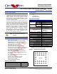
OV7725 Color CMOS VGA OmniPixel2™ CAMERACHIP™ Sensor
O
mni ision
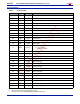
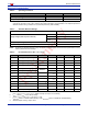
Table 5 Functional and AC Characteristics (-20°C < T
A
< 70°C)
Symbol Parameter Min Typ Max Unit
Functional Characteristics
A/D Differential non-linearity +
1/2 LSB
A/D Integral non-linearity +
1LSB
AGC Range 30 dB
Red/Blue adjustment range 12 dB
Inputs (PWDN, CLK, RESET#)
f
CLK
Input clock frequency 10 24 48 MHz
t
CLK
Input clock period 21 42 100 ns
t
CLK:DC
Clock duty cycle 45 50 55 %
t
S:RESET
Setting time after software/hardware reset 1 ms
t
S:REG
Settling time for register change (10 frames required) 300 ms
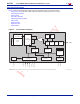
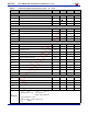
SCCB Timing (see Figure 4)
f
SCL
Clock frequency 400 KHz
t
LOW
Clock low period 1.3 µs
t
HIGH
Clock high period 600 ns
t
AA
SCL low to data out valid 100 900 ns
t
BUF
Bus free time before new START 1.3 µs
t
HD:STA
START condition hold time 600 ns
t
SU:STA
START condition setup time 600 ns
t
HD:DAT
Data in hold time 0 µs
t
SU:DAT
Data in setup time 100 ns
t
SU:STO
STOP condition setup time 600 ns
t
R,
t
F
SCCB rise/fall times 300 ns
t
DH
Data out hold time 50 ns
Outputs (VSYNC, HREF, PCLK, and D[9:0] (see Figure 5, Figure 6, Figure 7, and Figure 8)
t
PDV
PCLK[↓] to data out Valid 5 ns
t
SU
D[9:0] setup time 15 ns
t
HD
D[9:0] Hold time 8 ns
t
PHH
PCLK[↓] to HREF[↑]05ns
t
PHL
PCLK[↓] to HREF[↓]05ns
AC
Conditions:
• V
DD
: V
DD-C
= 1.8V, V
DD-A
= 3.3V, V
DD-IO
= 3.3V
• Rise/Fall Times: I/O: 5ns, Maximum
SCCB: 300ns, Maximum
• Input Capacitance: 10pf
• Output Loading: 25pF, 1.2KΩ to 3.3V
• f
CLK
: 24MHz