
Data Sheet
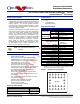

Electrical Characteristics
Version 1.1, March 30, 2007 Proprietary to OmniVision Technologies, Inc. 5
O
mni ision
Electrical Characteristics
NOTE: Exceeding the Absolute Maximum ratings shown above invalidates all AC and DC electrical specifications and may
result in permanent device damage.
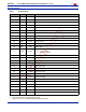
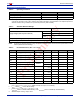
Table 2 Operating Conditions
Parameter Min Max
Operating temperature -20°C +70°C
Storage temperature
a
a. Exceeding the stresses listed may permanently damage the device. This is a stress rating only and functional operation
of the sensor at these and any other condition above those indicated in this specification is not implied. Exposure to
absolute maximum rating conditions for any extended period may affect reliability.
-40°C +125°C
Table 3 Absolute Maximum Ratings
Ambient Storage Temperature -40ºC to +95ºC
Supply Voltages (with respect to Ground)
V
DD-A
4.5 V
V
DD-C
3 V
V
DD-IO
4.5 V
All Input/Output Voltages (with respect to Ground) -0.3V to V
DD-IO
+0.5V
Lead-free Temperature, Surface-mount process 245ºC
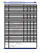
Table 4 DC Characteristics (-20°C < T
A
< 70°C)
Symbol Parameter Condition Min Typ Max Unit
V
DD-A
DC supply voltage – analog – 3.0 3.3 3.6 V
V
DD-C
DC supply voltage – digital core – 1.62 1.8 1.98 V
V
DD-IO
DC supply voltage – I/O – 2.5 – 3.3 V
I
DDA
Active (operating) current See Note
a
a. At 25ºC, V
DD-A
= 3.3V, V
DD-C
= 1.8V, V
DD-IO
= 3.3V
I
DDA
= ∑{I
DD-IO
+ I
DD-C
+ I
DD-A
}, f
CLK
= 24MHz at 30 fps YUV output, no I/O loading
10 + 8
b
b. I
DD-C
= 10mA, I
DD-A
= 8mA, without loading
mA
I
DDS-SCCB
Standby current
See Note
c
c. At 25ºC, V
DD-A
= 3.3V, V
DD-C
= 1.8V, V
DD-IO
= 3.3V
I
DDS-SCCB
refers to a SCCB-initiated Standby, while I
DDS-PWDN
refers to a PWDN pin-initiated Standby
1mA
I
DDS-PWDN
Standby current 10 20 µA
V
IH
Input voltage HIGH CMOS 0.7 x V
DD-IO
V
V
IL
Input voltage LOW 0.3 x V
DD-IO
V
V
OH
Output voltage HIGH CMOS 0.9 x V
DD-IO
V
V
OL
Output voltage LOW 0.1 x V
DD-IO
V
I
OH
Output current HIGH See Note
d
d. Standard Output Loading = 25pF, 1.2KΩ
8mA
I
OL
Output current LOW 15 mA
I
L
Input/Output leakage GND to V
DD-IO
± 1 µA