
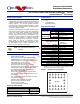
Data Sheet

Functional Description
Version 1.1, March 30, 2007 Proprietary to OmniVision Technologies, Inc. 3
O
mni ision
Image Sensor Array
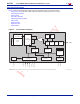
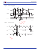
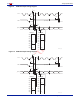
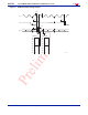
The OV7725 sensor has an image array of 656 x 488
pixels for a total of 320,128 pixels, of which 640 x 480
pixels are active (307,200 pixels). Figure 3 shows a
cross-section of the image sensor array.
Figure 3 Image Sensor Array
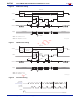
Timing Generator
In general, the timing generator controls the following
functions:
• Array control and frame generation
• Internal timing signal generation and distribution
• Frame rate timing
• Automatic Exposure Control (AEC)
• External timing outputs (VSYNC, HREF/HSYNC, and
PCLK)
Analog Signal Processor
This block performs all analog image functions including:
• Automatic Gain Control (AGC)
• Automatic White Balance (AWB)
A/D Converters
After the Analog Processing block, the bayer pattern Raw
signal is fed to a 10-bit analog-to-digital (A/D) converter
shared by G and BR channels. This A/D converter
operates at speeds up to 12 MHz and is fully synchronous
to the pixel rate (actual conversion rate is related to the
frame rate).
In addition to the A/D conversion, this block also has the
following functions:
• Digital Black-Level Calibration (BLC)
• Optional U/V channel delay
• Additional A/D range controls
blue
green
microlens
glass
microlensmicrolens
red
7725CSP_DS_003
In general, the combination of the A/D Range Multiplier
and A/D Range Control sets the A/D range and maximum
value to allow the user to adjust the final image brightness
as a function of the individual application.
Test Pattern Generator
The Test Pattern Generator features the following:
• 8-bar color bar pattern
• Shift "1" in output pin
Digital Signal Processor (DSP)
This block controls the interpolation from Raw data to
RGB and some image quality control.
• Edge enhancement (a two-dimensional high pass
filter)
• Color space converter (can change Raw data to RGB
or YUV/YCbCr)
• RGB matrix to eliminate color cross talk
• Hue and saturation control
• Programmable gamma control
• Transfer 10-bit data to 8-bit
Image Scaler
This block controls all output and data formatting required
prior to sending the image out. This block scales
YUV/RGB output from VGA to CIF and almost any size
under CIF.
Digital Video Port
Register bits COM2[1:0] increase I
OL
/I
OH
drive current
and can be adjusted as a function of the customer’s
loading.
SCCB Interface
The Serial Camera Control Bus (SCCB) interface controls
the C
AMERACHIP sensor operation. Refer to OmniVision
Technologies Serial Camera Control Bus (SCCB)
Specification for detailed usage of the serial control port.