
Data Sheet


Register Set
Version 1.1, March 30, 2007 Proprietary to OmniVision Technologies, Inc. 19
O
mni ision
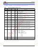
64 DSP_Ctrl1 1F RW
DSP Control Byte 1
Bit[7]: FIFO enable/disable selection
Bit[6]: UV adjust function ON/OFF selection
Bit[5]: SDE enable
Bit[4]: Color matrix ON/OFF selection
Bit[3]: Interpolation ON/OFF selection
Bit[2]: Gamma function ON/OFF selection
Bit[1]: Black defect auto correction ON/OFF
Bit[0]: White defect auto correction ON/OFF
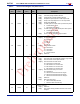
65 DSP_Ctrl2 00 RW
DSP Control Byte 2
Bit[7:4]: Reserved
Bit[3]: Vertical DCW enable
Bit[2]: Horizontal DCW enable
Bit[1]: Vertical zoom out enable
Bit[0]: Horizontal zoom out enable
66 DSP_Ctrl3 10 RW
DSP Control Byte 3
Bit[7]: UV output sequence option
Bit[6]: Reserved
Bit[5]: DSP color bar ON/OFF selection
Bit[4]: Reserved
Bit[3]: FIFO power down ON/OFF selection
Bit[2]: Scaling module power down control 1
Bit[1]: Scaling module power down control 2
Bit[0]: Interpolation module power down control
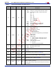
67 DSP_Ctrl4 00 RW
DSP Control Byte 4
Bit[7:3]: Reserved
Bit[2]: AEC selection
0: Before gamma
1: After gamma
Bit[1:0]: Output selection
00: YUV or RGB
01: YUV or RGB
10: RAW8
11: RAW10
68 AWB_bias 00 RW AWB BLC Level Clip
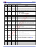
69 AWBCtrl1 5C RW
AWB Control 1
Bit[7:4]: Reserved
Bit[3]: G gain enable
0: AWB adjusts R and G gain
1: AWB adjusts R, G, and B gain
Bit[2]: Max color gain
0: Max color gain is 2x
1: Max color gain is 4x
Bit[1:0]: Reserved
Table 6 Device Control Register List (Sheet 9 of 13)
Address
(Hex)
Register
Name
Default
(Hex)
R/W Description