
Data Sheet


16 Proprietary to OmniVision Technologies, Inc. Version 1.1, March 30, 2007
OV7725 Color CMOS VGA OmniPixel2™ CAMERACHIP™ Sensor
O
mni ision
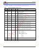
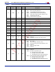
32 HREF 00 RW
Image Start and Size Control
Bit[7]: Mirror image edge alignment
Bit[6]: Vertical HREF window start control LSB
Bit[5:4]: Horizontal HREF window start control LSBs
Bit[3]: Data output bit shift test pattern ON/OFF control
Bit[2]: Vertical sensor size LSB
Bit[1:0]: Horizontal sensor size 2 LSBs
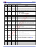
33 DM_LNL 00 RW Dummy Row Low 8 Bits
34 DM_LNH 00 RW Dummy Row High 8 Bits
35 ADoff_B 80 RW AD Offset Compensation Value for B Channel
36 ADoff_R 80 RW AD Offset Compensation Value for R Channel
37 ADoff_Gb 80 RW AD Offset Compensation Value for Gb Channel
38 ADoff_Gr 80 RW AD Offset Compensation Value for Gr Channel
39 Off_B 80 RW Analog Process B Channel Offset Compensation Value
3A Off_R 80 RW Analog Process R Channel Offset Compensation Value
3B Off_Gb 80 RW Analog Process Gb Channel Offset Compensation Value
3C Off_Gr 80 RW Analog Process Gr Channel Offset Compensation Value
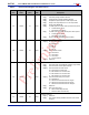
3D COM12 80 RW
Common Control 12
Bit[7:6]: Reserved
Bit[5:0]: DC offset compensation for analog process
3E COM13 E2 RW
Common Control 13
Bit[7]: BLC enable
Bit[6]: ADC channel BLC ON/OFF control
Bit[5]: Analog processing channel BLC ON/OFF control
Bit[4:3]: Reserved
Bit[2]: ABLC gain trigger enable
Bit[1:0]: Reserved
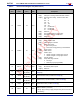
3F COM14 1F RW
Edge Enhancement Adjustment
Bit[7:4]: Reserved
Bit[3:2]: AD offset compensation option
x0: Use R/Gr channel value for B/Gb
01: Use B/Gb channel value for R/Gr
11: Use B/Gb/R/Gr channel value independently
Bit[1:0]: Analog processing offset compensation option
x0: Use R/Gr channel value for B/Gb
01: Use B/Gb channel value for R/Gr
11: Use B/Gb/R/Gr channel value independently
Table 6 Device Control Register List (Sheet 6 of 13)
Address
(Hex)
Register
Name
Default
(Hex)
R/W Description