
Data Sheet


Register Set
Version 1.1, March 30, 2007 Proprietary to OmniVision Technologies, Inc. 15
O
mni ision
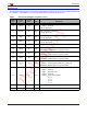
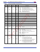
1C MIDH 7F R Manufacturer ID Byte – High (Read only = 0x7F)
1D MIDL A2 R Manufacturer ID Byte – Low (Read only = 0xA2)
1E RSVD XX – Reserved
1F LAEC 00 RW Fine AEC Value - defines exposure value less than one row period
20 COM11 10 RW
Common Control 11
Bit[7:2]: Reserved
Bit[1]: Single frame ON/OFF selection
Bit[0]: Single frame transfer trigger
21 RSVD XX – Reserved
22 BDBase FF RW Banding Filter Minimum AEC Value
23 BDMStep 01 RW Banding Filter Maximum Step
24 AEW 75 RW AGC/AEC - Stable Operating Region (Upper Limit)
25 AEB 63 RW AGC/AEC - Stable Operating Region (Lower Limit)
26 VPT D4 RW
AGC/AEC Fast Mode Operating Region
Bit[7:4]: High nibble of upper limit of fast mode control zone
Bit[3:0]: High nibble of lower limit of fast mode control zone
27 RSVD XX – Reserved
28 REG28 00 RW
Register 28
Bit[7:1]: Reserved
Bit[0]: Selection on the number of dummy rows, N
29 HOutSize
A0 (VGA)
50 (QVGA)
RW Horizontal Data Output Size MSBs (2 LSBs at register EXHCH[1:0])
2A EXHCH 00 RW
Dummy Pixel Insert MSB
Bit[7:4]: 4 MSB for dummy pixel insert in horizontal direction
Bit[3]: Reserved
Bit[2]: Vertical data output size LSB
Bit[1:0]: Horizontal data output size 2 LSBs
2B EXHCL 00 RW
Dummy Pixel Insert LSB
8 LSB for dummy pixel insert in horizontal direction
2C VOutSize
F0 (VGA)
78 (QVGA)
RW Vertical Data Output Size MSBs (LSB at register EXHCH[2])
2D ADVFL 00 RW LSB of Insert Dummy Rows in Vertical Sync (1 bit equals 1 row)
2E ADVFH 00 RW MSB of Insert Dummy Rows in Vertical Sync
2F YAVE 00 RW Y/G Channel Average Value
30 LumHTh 80 RW Histogram AEC/AGC Luminance High Level Threshold
31 LumLTh 60 RW Histogram AEC/AGC Luminance Low Level Threshold
Table 6 Device Control Register List (Sheet 5 of 13)
Address
(Hex)
Register
Name
Default
(Hex)
R/W Description