
Data Sheet


14 Proprietary to OmniVision Technologies, Inc. Version 1.1, March 30, 2007
OV7725 Color CMOS VGA OmniPixel2™ CAMERACHIP™ Sensor
O
mni ision
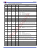
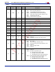
14 COM9 4A RW
Common Control 9
Bit[7]: Histogram or average based AEC/AGC selection
Bit[6:4]: Automatic Gain Ceiling - maximum AGC value
000: 2x
001: 4x
010: 8x
011: 16x
100: 32x
101 Not allowed
110: Not allowed
111: Not allowed
Bit[3]: Reserved
Bit[2]: Drop VSYNC output of corrupt frame
Bit[1]: Drop HREF output of corrupt frame
Bit[0]: Reserved
15 COM10 00 RW
Common Control 10
Bit[7]: Output negative data
Bit[6]: HREF changes to HSYNC
Bit[5]: PCLK output option
0: Free running PCLK
1: PCLK does not toggle during horizontal blank
Bit[4]: PCLK reverse
Bit[3]: HREF reverse
Bit[2]: VSYNC option
0: VSYNC changes on falling edge of PCLK
1: VSYNC changes on rising edge of PCLK
Bit[1]: VSYNC negative
Bit[0]: Output data range selection
0: Full range
1: Data from [10] to [F0] (8 MSBs)
16 REG16 00 RW
Register 16
Bit[7]: Bit shift test pattern options
Bit[6:0]: Reserved
17 HSTART
23 (VGA)
3F (QVGA)
RW
Horizontal Frame (HREF column) Start 8 MSBs (2 LSBs are at
HREF[5:4])
18 HSIZE
A0 (VGA)
50 (QVGA)
RW Horizontal Sensor Size (2 LSBs are at HREF[1:0])
19 VSTRT
07 (VGA)
03 (QVGA)
RW Vertical Frame (row) Start 8 MSBs (1 LSB is at HREF[6])
1A VSIZE
F0 (VGA)
78 (QVGA)
RW Vertical Sensor Size (1 LSB is at HREF[2])
1B PSHFT 40 RW
Data Format - Pixel Delay Select (delays timing of the D[9:0] data
relative to HREF in pixel units)
• Range: [00] (no delay) to [FF] (256 pixel delay which accounts for
whole array)
Table 6 Device Control Register List (Sheet 4 of 13)
Address
(Hex)
Register
Name
Default
(Hex)
R/W Description