
Data Sheet


Register Set
Version 1.1, March 30, 2007 Proprietary to OmniVision Technologies, Inc. 13
O
mni ision
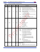
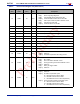
10 AEC 40 RW
Exposure Value
Bit[7:0]: AEC[7:0] (see register AECH for AEC[15:8])
11 CLKRC 80 RW
Internal Clock
Bit[7]: Reserved
Bit[6]: Use external clock directly (no clock pre-scale
available)
Bit[5:0]: Internal clock pre-scalar
F(internal clock) = F(input clock)/(Bit[5:0]+1)/2
• Range: [0 0000] to [1 1111]
12 COM7 00 RW
Common Control 7
Bit[7]: SCCB Register Reset
0: No change
1: Resets all registers to default values
Bit[6]: Resolution selection
0: VGA
1: QVGA
Bit[5]: BT.656 protocol ON/OFF selection
Bit[4]: Sensor RAW
Bit[3:2]: RGB output format control
00: GBR4:2:2
01: RGB565
10: RGB555
11: RGB444
Bit[1:0]: Output format control
00: YUV
01: Processed Bayer RAW
10: RGB
11: Bayer RAW
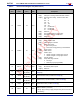
13 COM8 8F RW
Common Control 8
Bit[7]: Enable fast AGC/AEC algorithm
Bit[6]: AEC - Step size limit
0: Step size is limited to vertical blank
1: Unlimited step size
Bit[5]: Banding filter ON/OFF
Bit[4]: Enable AEC below banding value
Bit[3]: Fine AEC ON/OFF control
Bit[2]: AGC Enable
Bit[1]: AWB Enable
Bit[0]: AEC Enable
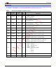
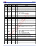
Table 6 Device Control Register List (Sheet 3 of 13)
Address
(Hex)
Register
Name
Default
(Hex)
R/W Description