
Data Sheet


12 Proprietary to OmniVision Technologies, Inc. Version 1.1, March 30, 2007
OV7725 Color CMOS VGA OmniPixel2™ CAMERACHIP™ Sensor
O
mni ision
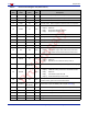
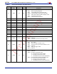
0C COM3 10 RW
Common Control 3
Bit[7]: Vertical flip image ON/OFF selection
Bit[6]: Horizontal mirror image ON/OFF selection
Bit[5]: Swap B/R output sequence in RGB output mode
Bit[4]: Swap Y/UV output sequence in YUV output mode
Bit[3]: Swap output MSB/LSB
Bit[2]: Tri-state option for output clock at power-down period
0: Tri-state at this period
1: No tri-state at this period
Bit[1]: Tri-state option for output data at power-down period
0: Tri-state at this period
1: No tri-state at this period
Bit[0]: Sensor color bar test pattern output enable
0D COM4 41 RW
Common Control 4
Bit[7:6]: PLL frequency control
00: Bypass PLL
01: PLL 4x
10: PLL 6x
11: PLL 8x
Bit[5:4]: AEC evaluate window
00: Full window
01: 1/2 window
10: 1/4 window
11: Low 2/3 window
Bit[3:0]: Reserved
0E COM5 01 RW
Common Control 5
Bit[7]: Auto frame rate control ON/OFF selection (night mode)
Bit[6]: Auto frame rate control speed selection
Bit[5:4]: Auto frame rate max rate control
00: No reduction of frame rate
01: Max reduction to 1/2 frame rate
10: Max reduction to 1/4 frame rate
11: Max reduction to 1/8 frame rate
Bit[3:2]: Auto frame rate active point control
00: Not allowed
01: Add frame when AGC reaches 4x gain
10: Add frame when AGC reaches 8x gain
11: Add frame when AGC reaches 16x gain
Bit[1]: Reserved
Bit[0]: AEC max step control
0: AEC increase step has limit
1: No limit to AEC increase step
0F COM6 43 RW
Common Control 6
Bit[7:1]: Reserved
Bit[0]: Auto window setting ON/OFF selection when format
changes
Table 6 Device Control Register List (Sheet 2 of 13)
Address
(Hex)
Register
Name
Default
(Hex)
R/W Description