
Data Sheet


Register Set
Version 1.1, March 30, 2007 Proprietary to OmniVision Technologies, Inc. 11
O
mni ision
Register Set
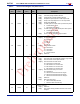
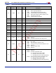
Table 6 provides a list and description of the Device Control registers contained in the OV7725. For all register Enable/Disable
bits, ENABLE = 1 and DISABLE = 0. The device slave addresses are 42 for write and 43 for read.
Table 6 Device Control Register List (Sheet 1 of 13)
Address
(Hex)
Register
Name
Default
(Hex)
R/W Description
00 GAIN 00 RW
AGC – Gain control gain setting
Bit[7:0]: AGC[7:0]
• Range: [00] to [FF]
01 BLUE 80 RW
AWB – Blue channel gain setting
• Range: [00] to [FF]
02 RED 80 RW
AWB – Red channel gain setting
• Range: [00] to [FF]
03 GREEN 00 RW
AWB – Green channel gain setting
• Range: [00] to [FF]
04 RSVD XX – Reserved
05 BAVG 00 RW
U/B Average Level
Automatically updated based on chip output format
06 GAVG 00 RW
Y/Gb Average Level
Automatically updated based on chip output format
07 RAVG 00 RW
V/R Average Level
Automatically updated based on chip output format
08 AECH 00 RW
Exposure Value – AEC MSBs
Bit[7:0]: AEC[15:8] (see register AEC for AEC[7:0]}
Automatically updated based on chip output format
09 COM2 01 RW
Common Control 2
Bit[7:5]: Reserved
Bit[4]: Soft sleep mode
Bit[3:2]: Reserved
Bit[1:0]: Output drive capability
00: 1x
01: 2x
10: 3x
11: 4x
0A PID 77 R Product ID Number MSB (Read only)
0B VER 21 R Product ID Number LSB (Read only)