
Data Sheet
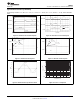

IN
GND
EN NR/FB
OUT1
2
3 4
5
TPS731
www.ti.com
SBVS034N –SEPTEMBER 2003–REVISED DECEMBER 2015
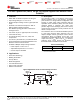
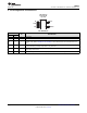
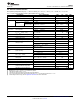
5 Pin Configuration and Functions
DBV Package
5-Pin SOT-23
Top View
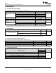
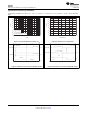
Pin Functions
PIN
I/O DESCRIPTION
NAME NO.
IN 1 I Input supply.
GND 2 — Ground.
Driving the enable pin (EN) high turns on the regulator. Driving this pin low puts the regulator into
EN 3 I shutdown mode. Refer to Enable Pin and Shutdown for more details. EN can be connected to IN if not
used.
Fixed-voltage versions only—connecting an external capacitor to this pin bypasses noise generated by
NR 4 —
the internal bandgap, reducing output noise to very low levels.
Adjustable-voltage version only—this is the input to the control loop error amplifier, and is used to set the
FB 4 I
output voltage of the device.
OUT 5 O Output of the regulator. There are no output capacitor requirements for stability.
Copyright © 2003–2015, Texas Instruments Incorporated Submit Documentation Feedback 3
Product Folder Links: TPS731