
Data Sheet


D IN OUT OUT
P (V V ) I= - ´
TPS731
SBVS034N –SEPTEMBER 2003–REVISED DECEMBER 2015
www.ti.com
Thermal Considerations (continued)
10.3.1 Power Dissipation
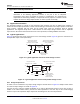
The ability to remove heat from the die is different for each package type, presenting different considerations in
the PCB layout. The PCB area around the device that is free of other components moves the heat from the
device to the ambient air. Performance data for JEDEC low- and high-K boards are shown in the Thermal
Information table. Using heavier copper will increase the effectiveness in removing heat from the device.
Power dissipation depends on input voltage and load conditions. Power dissipation (P
D
) is equal to the product of
the output current times the voltage drop across the output pass element (V
IN
to V
OUT
):
(6)
Power dissipation can be minimized by using the lowest possible input voltage necessary to assure the required
output voltage.
18 Submit Documentation Feedback Copyright © 2003–2015, Texas Instruments Incorporated
Product Folder Links: TPS731