
Data Sheet


EN
V
OUT
V
IN
GND
PLANE
TPS731
C
OUT
GND
PLANE
R
1
R
2
C
IN
TPS731
www.ti.com
SBVS034N –SEPTEMBER 2003–REVISED DECEMBER 2015
9 Power Supply Recommendations
These devices are designed to operate from an input voltage supply range between 1.7 V and 5.5 V. The input
voltage range provides adequate headroom in order for the device to have a regulated output. This input supply
must be well regulated. If the input supply is noisy, additional input capacitors with low ESR can help improve the
output noise performance.
10 Layout
10.1 Layout Guidelines
To improve AC performance such as PSRR, output noise, and transient response, it is recommended that the
PCB be designed with separate ground planes for V
IN
and V
OUT
, with each ground plane connected only at the
ground pin (GND) of the device. In addition, the ground connection for the bypass capacitor should connect
directly to the GND pin of the device.
Solder pad footprint recommendations for the TPS731xx are presented in Application Bulletin Solder Pad
Recommendations for Surface-Mount Devices (SBFA015), available from the TI website at www.ti.com.
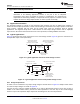
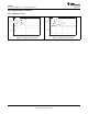
10.2 Layout Example
Figure 35. Example Layout (DBV Package)
10.3 Thermal Considerations
Thermal protection disables the output when the junction temperature rises to approximately 160°C, allowing the
device to cool. When the junction temperature cools to approximately 140°C, the output circuitry is again
enabled. Depending on power dissipation, thermal resistance, and ambient temperature, the thermal protection
circuit may cycle on and off. This limits the dissipation of the regulator, protecting it from damage due to
overheating.
Any tendency to activate the thermal protection circuit indicates excessive power dissipation or an inadequate
heatsink. For reliable operation, junction temperature should be limited to 125°C maximum. To estimate the
margin of safety in a complete design (including heatsink), increase the ambient temperature until the thermal
protection is triggered; use worst-case loads and signal conditions. For good reliability, thermal protection should
trigger at least 35°C above the maximum expected ambient condition of your application. This produces a worst-
case junction temperature of 125°C at the highest expected ambient temperature and worst-case load.
The internal protection circuitry of the TPS731xx has been designed to protect against overload conditions. It
was not intended to replace proper heatsinking. Continuously running the TPS731xx into thermal shutdown
degrades device reliability.
Copyright © 2003–2015, Texas Instruments Incorporated Submit Documentation Feedback 17
Product Folder Links: TPS731