
Data Sheet

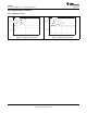


OUT
OUT 1 2 LOAD
V
dV / dt
C 80k (R R ) R
=
´ W +P P
OUT
OUT LOAD
V
dV / dt
C 80k R
=
´ W P
TPS731
www.ti.com
SBVS034N –SEPTEMBER 2003–REVISED DECEMBER 2015
Typical Applications (continued)
8.2.2 Detailed Design Procedure
8.2.2.1 Input and Output Capacitor Requirements
Although an input capacitor is not required for stability, it is good analog design practice to connect a 0.1-μF to
1-μF, low ESR capacitor across the input supply near the regulator. This counteracts reactive input sources and
improves transient response, noise rejection, and ripple rejection. A higher-value capacitor may be necessary if
large, fast rise-time load transients are anticipated or the device is located several inches from the power source.
8.2.2.2 Dropout Voltage
The TPS731xx uses an NMOS pass transistor to achieve extremely low dropout. When (V
IN
– V
OUT
) is less than
the dropout voltage (V
DO
), the NMOS pass device is in its linear region of operation and the input-to-output
resistance is the R
DS(on)
of the NMOS pass element.
For large step changes in load current, the TPS731xx requires a larger voltage drop from V
IN
to V
OUT
to avoid
degraded transient response. The boundary of this transient dropout region is approximately twice the DC
dropout. Values of V
IN
– V
OUT
above this line insure normal transient response.
Operating in the transient dropout region can cause an increase in recovery time. The time required to recover
from a load transient is a function of the magnitude of the change in load current rate, the rate of change in load
current, and the available headroom (V
IN
to V
OUT
voltage drop). Under worst-case conditions [full-scale
instantaneous load change with (V
IN
– V
OUT
) close to DC dropout levels], the TPS731xx can take a couple of
hundred microseconds to return to the specified regulation accuracy.
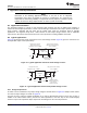
8.2.2.3 Transient Response
The low open-loop output impedance provided by the NMOS pass element in a voltage follower configuration
allows operation without an output capacitor for many applications. As with any regulator, the addition of a
capacitor (nominal value 1 μF) from the output pin (OUT) to ground will reduce undershoot magnitude but
increase its duration. In the adjustable version, the addition of a capacitor, C
FB
, from the OUT pin to the FB pin
will also improve the transient response.
The TPS731xx does not have active pulldown when the output is overvoltage. This allows applications that
connect higher voltage sources, such as alternate power supplies, to the output. This also results in an output
overshoot of several percent if the load current quickly drops to zero when a capacitor is connected to the output.
The duration of overshoot can be reduced by adding a load resistor. The overshoot decays at a rate determined
by output capacitor C
OUT
and the internal and external load resistance. The rate of decay is given by Equation 4
and Equation 5:
(Fixed-voltage version)
(4)
(Adjustable-voltage version)
(5)
Copyright © 2003–2015, Texas Instruments Incorporated Submit Documentation Feedback 15
Product Folder Links: TPS731