
Data Sheet


TPS73101
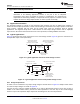
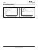
GNDEN FB
IN OUT
V
IN
V
OU
T
V
OUT
= x1.204
(R
1
+ R
2
)
R
2
R
1
C
FB
R
2
Optionalinputcapacitor.
Mayimprovesource
impedance,noise,orPSRR.
Optionaloutputcapacitor.
Mayimproveloadtransient,
noise,orPSRR.
Optionalcapacitor
reducesoutputnoise
andimproves
transientresponse.
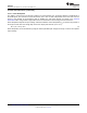
OFF
ON
TPS731xx
GNDEN
ON
OFF
NR
IN OUT
VIN VOUT
Optionalinputcapacitor.
Mayimprovesource
impedance,noise,orPSRR.
Optionaloutputcapacitor.
Mayimproveloadtransient,
noise,orPSRR.
Optionalbypass
capacitortoreduce
outputnoise.
TPS731
SBVS034N –SEPTEMBER 2003–REVISED DECEMBER 2015
www.ti.com
8 Application and Implementation
NOTE
Information in the following applications sections is not part of the TI component
specification, and TI does not warrant its accuracy or completeness. TI’s customers are
responsible for determining suitability of components for their purposes. Customers should
validate and test their design implementation to confirm system functionality.
8.1 Application Information
The TPS731xx belongs to a family of new generation LDO regulators that use an NMOS pass transistor to
achieve ultra-low-dropout performance, reverse current blockage, and freedom from output capacitor constraints.
These features, combined with low noise and an enable input, make the TPS731xx ideal for portable
applications. This regulator family offers a wide selection of fixed output voltage versions and an adjustable
output version. All versions have thermal and over-current protection, including foldback current limit.
8.2 Typical Applications
Figure 31 shows the basic circuit connections for the fixed-voltage models. Figure 32 gives the connections for
the adjustable output version (TPS73101).
Figure 31. Typical Application Circuit for Fixed-Voltage Versions
Figure 32. Typical Application Circuit for Adjustable-Voltage Version
8.2.1 Design Requirements
R
1
and R
2
can be calculated for any output voltage using the formula shown in Figure 32. Sample resistor values
for common output voltages are shown in Figure 30.
For best accuracy, make the parallel combination of R
1
and R
2
approximately equal to 19 kΩ. This 19 kΩ, in
addition to the internal 8-kΩ resistor, presents the same impedance to the error amp as the 27-kΩ bandgap
reference output. This impedance helps compensate for leakages into the error amp terminals.
14 Submit Documentation Feedback Copyright © 2003–2015, Texas Instruments Incorporated
Product Folder Links: TPS731