
Data Sheet

TIP31G, TIP31AG, TIP31BG, TIP31CG (NPN), TIP32G, TIP32AG, TIP32BG,
TIP32CG (PNP)
www.onsemi.com
2
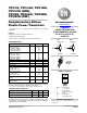
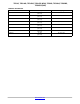
ELECTRICAL CHARACTERISTICS (T
C
= 25°C unless otherwise noted)
Characteristic
Symbol Min Max Unit
OFF CHARACTERISTICS
Collector−Emitter Sustaining Voltage (Note 2)
(I
C
= 30 mAdc, I
B
= 0)
TIP31G, TIP32G
TIP31AG, TIP32AG
TIP31BG, TIP32BG
TIP31CG, TIP32CG
V
CEO(sus)
40
60
80
100
−
−
−
−
Vdc
Collector Cutoff Current
(V
CE
= 30 Vdc, I
B
= 0)
TIP31G, TIP32G, TIP31AG, TIP32AG
(V
CE
= 60 Vdc, I
B
= 0)
TIP31BG, TIP31CG, TIP32BG, TIP32CG
I
CEO
−
−
0.3
0.3
mAdc
Collector Cutoff Current
(V
CE
= 40 Vdc, V
EB
= 0)
TIP31G, TIP32G
(V
CE
= 60 Vdc, V
EB
= 0)
TIP31AG, TIP32AG
(V
CE
= 80 Vdc, V
EB
= 0)
TIP31BG, TIP32BG
(V
CE
= 100 Vdc, V
EB
= 0)
TIP31CG, TIP32CG
I
CES
−
−
−
−
200
200
200
200
mAdc
Emitter Cutoff Current
(V
BE
= 5.0 Vdc, I
C
= 0)
I
EBO
− 1.0
mAdc
ON CHARACTERISTICS (Note 2)
DC Current Gain
(I
C
= 1.0 Adc, V
CE
= 4.0 Vdc)
(I
C
= 3.0 Adc, V
CE
= 4.0 Vdc)
h
FE
25
10
−
50
−
Collector−Emitter Saturation Voltage
(I
C
= 3.0 Adc, I
B
= 375 mAdc)
V
CE(sat)
− 1.2
Vdc
Base−Emitter On Voltage
(I
C
= 3.0 Adc, V
CE
= 4.0 Vdc)
V
BE(on)
− 1.8
Vdc
DYNAMIC CHARACTERISTICS
Current−Gain − Bandwidth Product
(I
C
= 500 mAdc, V
CE
= 10 Vdc, f
test
= 1.0 MHz)
f
T
3.0 −
MHz
Small−Signal Current Gain
(I
C
= 0.5 Adc, V
CE
= 10 Vdc, f = 1.0 kHz)
h
fe
20 −
−
Product parametric performance is indicated in the Electrical Characteristics for the listed test conditions, unless otherwise noted. Product
performance may not be indicated by the Electrical Characteristics if operated under different conditions.
2. Pulse Test: Pulse Width ≤ 300 ms, Duty Cycle ≤ 2.0%.