
Data Sheet

TIP110, TIP111, TIP112 (NPN); TIP115, TIP116, TIP117 (PNP)
www.onsemi.com
2
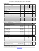
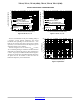
MAXIMUM RATINGS
Rating Symbol
TIP110,
TIP115
TIP111,
TIP116
TIP112,
TIP117
Unit
Collector−Emitter Voltage V
CEO
60 80 100 Vdc
Collector−Base Voltage V
CB
60 80 100 Vdc
Emitter−Base Voltage V
EB
5.0 Vdc
Collector Current − Continuous
− Peak
I
C
2.0
4.0
Adc
Base Current I
B
50 mAdc
Total Power Dissipation @ T
C
= 25°C
Derate above 25°C
P
D
50
0.4
W
W/°C
Total Power Dissipation @ T
A
= 25°C
Derate above 25°C
P
D
2.0
0.016
W
W/°C
Unclamped Inductive Load Energy − Figure 13 E 25 mJ
Operating and Storage Junction T
J
, T
stg
–65 to +150 °C
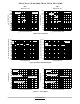
THERMAL CHARACTERISTICS
Characteristics Symbol Max Unit
Thermal Resistance, Junction−to−Case
R
q
JC
2.5 °C/W
Thermal Resistance, Junction−to−Ambient
R
q
JA
62.5 °C/W
Stresses exceeding those listed in the Maximum Ratings table may damage the device. If any of these limits are exceeded, device functionality
should not be assumed, damage may occur and reliability may be affected.
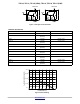
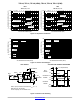
ELECTRICAL CHARACTERISTICS (T
C
= 25°C unless otherwise noted)
Characteristic
Symbol Min Max Unit
OFF CHARACTERISTICS
Collector−Emitter Sustaining Voltage (Note 1)
(I
C
= 30 mAdc, I
B
= 0) TIP110, TIP115
TIP111, TIP116
TIP112, TIP117
V
CEO(sus)
60
80
100
−
−
−
Vdc
Collector Cutoff Current
(V
CE
= 30 Vdc, I
B
= 0) TIP110, TIP115
(V
CE
= 40 Vdc, I
B
= 0) TIP111, TIP116
(V
CE
= 50 Vdc, I
B
= 0) TIP112 ,TIP117
I
CEO
−
−
−
2.0
2.0
2.0
mAdc
Collector Cutoff Current
(V
CB
= 60 Vdc, I
E
= 0) TIP110, TIP115
(V
CB
= 80 Vdc, I
E
= 0) TIP111, TIP116
(V
CB
= 100 Vdc, I
E
= 0) TIP112, TIP117
I
CBO
−
−
−
1.0
1.0
1.0
mAdc
Emitter Cutoff Current
(V
BE
= 5.0 Vdc, I
C
= 0)
I
EBO
− 2.0 mAdc
ON CHARACTERISTICS (Note 1)
DC Current Gain
(I
C
= 1.0 Adc, V
CE
= 4.0 Vdc)
(I
C
= 2.0 Adc, V
CE
= 4.0 Vdc)
h
FE
1000
500
−
−
−
Collector−Emitter Saturation Voltage (I
C
= 2.0 Adc, I
B
= 8.0 mAdc) V
CE(sat)
− 2.5 Vdc
Base−Emitter On Voltage (I
C
= 2.0 Adc, V
CE
= 4.0 Vdc) V
BE(on)
− 2.8 Vdc
DYNAMIC CHARACTERISTICS
Small−Signal Current Gain (I
C
= 0.75 Adc, V
CE
= 10 Vdc, f = 1.0 MHz) h
fe
25 − −
Output Capacitance
(V
CB
= 10 Vdc, I
E
= 0, f = 0.1 MHz) TIP115, TIP116, TIP117
TIP110, TIP111, TIP112
C
ob
−
−
200
100
pF
Product parametric performance is indicated in the Electrical Characteristics for the listed test conditions, unless otherwise noted. Product
performance may not be indicated by the Electrical Characteristics if operated under different conditions.
1. Pulse Test: Pulse Width v 300 ms, Duty Cycle v 2%.