
Datasheet


NCP3063, NCP3063B, NCV3063
http://onsemi.com
9
(See Notes 9, 10, 11)
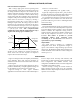
Step−Down Step−Up Voltage−Inverting
t
on
t
off
V
out
) V
F
V
in
* V
SWCE
* V
out
V
out
) V
F
* V
in
V
in
* V
SWCE
|V
out
| ) V
F
V
in
* V
SWCE
t
on
t
on
t
off
f
ǒ
t
on
t
off
) 1
Ǔ
t
on
t
off
f
ǒ
t
on
t
off
) 1
Ǔ
t
on
t
off
f
ǒ
t
on
t
off
) 1
Ǔ
C
T
C
T
+
381.6 @ 10
*6
f
osc
* 343 @ 10
*12
I
L(avg)
I
out
I
out
ǒ
t
on
t
off
) 1
Ǔ
I
out
ǒ
t
on
t
off
) 1
Ǔ
I
pk
(Switch)
I
L(avg)
)
DI
L
2
I
L(avg)
)
DI
L
2
I
L(avg)
)
DI
L
2
R
SC
0.20
I
pk (Switch)
0.20
I
pk (Switch)
0.20
I
pk (Switch)
L
ǒ
V
in
* V
SWCE
* V
out
DI
L
Ǔ
t
on
ǒ
V
in
* V
SWCE
DI
L
Ǔ
t
on
ǒ
V
in
* V
SWCE
DI
L
Ǔ
t
on
V
ripple(pp)
DI
L
ǒ
1
8 f C
O
Ǔ
2
) (ESR)
2
Ǹ
[
t
on
I
out
C
O
) DI
L
@ ESR [
t
on
I
out
C
O
) DI
L
@ ESR
V
out
V
TH
ǒ
R
2
R
1
) 1
Ǔ
V
TH
ǒ
R
2
R
1
) 1
Ǔ
V
TH
ǒ
R
2
R
1
) 1
Ǔ
9. V
SWCE
− Darlington Switch Collector to Emitter Voltage Drop, refer to Figures 7, 8, 9 and 10.
10.V
F
− Output rectifier forward voltage drop. Typical value for 1N5819 Schottky barrier rectifier is 0.4 V.
11. The calculated t
on
/t
off
must not exceed the minimum guaranteed oscillator charge to discharge ratio.
The Following Converter Characteristics Must Be Chosen:
V
in
− Nominal operating input voltage.
V
out
− Desired output voltage.
I
out
− Desired output current.
DI
L
− Desired peak−to−peak inductor ripple current. For maximum output current it is suggested that DI
L
be chosen to be
less than 10% of the average inductor current I
L(avg)
. This will help prevent I
pk
(Switch)
from reaching the current limit threshold
set by R
SC
. If the design goal is to use a minimum inductance value, let DI
L
= 2(I
L(avg)
). This will proportionally reduce
converter output current capability.
f − Maximum output switch frequency.
V
ripple(pp)
− Desired peak−to−peak output ripple voltage. For best performance the ripple voltage should be kept to a low
value since it will directly affect line and load regulation. Capacitor C
O
should be a low equivalent series resistance (ESR)
electrolytic designed for switching regulator applications.
Figure 15. Design Equations