
Datasheet


NCP3063, NCP3063B, NCV3063
http://onsemi.com
16
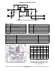
Figure 31. Typical Schematic of Buck Converter with RC Snubber and Pulse Feedback
IC1 NCP3063
5
36
4
8
7
1
2
R3
COMP
TC
GND
N.C. SWC
SWE
V
CC
I
PK
C1
0V 0V
C4
C2
R5
22k
R2
R1
L1
D1C3
R4
4n7
10R
In some cases where there are oscillations on the output
due to the input/output combination, output load variations
or PCB layout a snubber circuit on the SWE Pin will help
minimize the oscillation. Typical usage is shown in the
Figure 31. C3 values can be selected between 2.2 nF and
6.8 nF and R4 can be from 10 W to 22 W.
ORDERING INFORMATION
Device Package Shipping
†
NCP3063PG PDIP−8
(Pb−Free)
50 Units / Rail
NCP3063BPG PDIP−8
(Pb−Free)
50 Units / Rail
NCP3063BMNTXG DFN−8
(Pb−Free)
4000 / Tape & Reel
NCP3063DR2G SOIC−8
(Pb−Free)
2500 / Tape & Reel
NCP3063BDR2G SOIC−8
(Pb−Free)
2500 / Tape & Reel
NCP3063MNTXG DFN−8
(Pb−Free)
4000 / Tape & Reel
NCV3063PG PDIP−8
(Pb−Free)
50 Units / Rail
NCV3063DR2G SOIC−8
(Pb−Free)
2500 / Tape & Reel
NCV3063MNTXG DFN−8
(Pb−Free)
4000 / Tape & Reel
†For information on tape and reel specifications, including part orientation and tape sizes, please refer to our Tape and Reel Packaging
Specifications Brochure, BRD8011/D.
NCV prefix is for automotive and other applications requiring site and change control.