
Datasheet


NCP3063, NCP3063B, NCV3063
http://onsemi.com
15
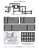
Figure 29. Typical Buck Application Schematic with External Low V
CE
(sat) PNP Transistor
IC1 NCP3063
5
36
4
8
7
1
2
R2
V
IN
= 8 − 19 V
V
OUT
= 3V3/1 A
+
COMP
TC
GND
N.C. SWC
SWE
V
CC
I
PK
1k
C2
100n
C1
0V GND
C5
100n
C6
C3
2n2
R5
33
R3 1k7
R1
150m
33m
L1
Q1 NSS35200
D2
NSR0130
+
R4
33
D1
1N5819
100m100m
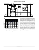
50
55
60
65
70
75
80
85
90
95
100
0 0.1 0.2 0.3 0.4 0.5 0.6 0.7 0.8 0.9 1
Figure 30. NCP3063 Efficiency vs. Output Current for
External Low V
CE(sat)
at V
in
= +5 V, f = 160 kHz,
T
A
= 255C
EFFICIENCY (%)
OUTPUT LOAD (Adc)
Typical application of the buck converter with external
bipolar transistor is shown in the Figure 29. It is an ideal
solution for configurations where the input and output
voltage difference is small and high efficiency is required.
NSS35200, the low V
CE
(
sat)
transistor from
ON Semiconductor will be ideal for applications with 1 A
output current, the input voltages up to 15 V and operating
frequency 100 − 150 kHz. The switching speed could be
improved by using desaturation diode D2.