
Datasheet


NCP3063, NCP3063B, NCV3063
http://onsemi.com
13
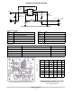
Figure 25. Typical Boost Application Schematic with External NMOS Transistor
IC1 NCP3063
5
36
4
8
7
1
2
R4
V
IN
= 8 − 18 V/0.6 A
V
OUT
= 31 V/0.35 A
+
COMP
TC
GND
N.C. SWC
SWE
V
CC
I
PK
1k
1N5819
D1
R3
M18
C2
100n
C1
0V GND
C6
100n
C7
R8
1k
C4
1n2
C5 6n8
R7
470
R5 24k
C3 10n
R2 1k
R1 82m
10m
L1
6
2
5
1
4
3
G
D
S
Q1
NTD18N06
IC2 BC846BPD
330m 330m
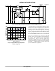
Figure 26. Typical Efficiency for Application
Shown in Figure 25.
70
72
74
76
78
80
82
84
86
6 8 10 12 14 16 18 20
70
72
74
76
78
80
82
84
86
6 8 10 12 14 16 18 20
EFFICIENCY (%)
INPUT VOLTAGE (V)
I
LOAD
= 350 mA
External transistor is recommended in applications where
wide input voltage ranges and higher power is required. The
suitable schematic with an additional NMOS transistor and
its driving circuit is shown in the Figure 25. The driving
circuit is controlled from SWE Pin of the NCP3063 through
frequency compensated resistor divider R7/R8. The driver
IC2 is ON Semiconductor low cost dual NPN/PNP
transistor BC846BPD. Its NPN transistor is connected as a
super diode for charging the gate capacitance. The PNP
transistor works as an emitter follower for discharging the
gate capacitor. This configuration assures sharp driving
edge between 50 − 100 ns as well as it limits power
consumption of R7/R8 divider down to 50 mW. The output
current limit is balanced by resistor R3. The fast switching
with low R
DS(on)
NMOS transistor will achieve efficiencies
up to 85% in automotive applications.