
Datasheet


NCP3063, NCP3063B, NCV3063
http://onsemi.com
12
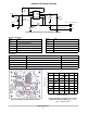
Figure 22. Typical Voltage Inverting Application Schematic
J504
GND
1
J503
1
C503
2.2 nF
C502
C501
R502
U501
NCP3063
5
36
4
8
7
1
2
COMP
TCAP
GND
N.C. SWC
SWE
R503
R501
0R15
L501
J502
GND
1
J501
1
+V
IN
= +5 V
0.1 mF
16K9 ±1%
1K96 ±1%
330 mF / 25 V
+
22 mH
V
OUT
= −12 V / 100 mA
V
CC
I
PK
D501
C505
470 mF / 35 V
+
C506
0.1 mF
1N5819
Value of Components
Name Value
L501
22 mH, I
sat
> 1.5 A
D501 1 A, 40 V Schottky Rectifier
C502
330 mF, 25 V, Low ESR
C505
470 mF, 35 V, Low ESR
C503 2.2 nF Ceramic Capacitor
Name Value
R501
150 mW, 0.5 W
R502
16.9 kW
R503
1.96 kW
C501 100 nF Ceramic Capacitor
C506 100 nF Ceramic Capacitor
Test Results
Test Condition Results
Line Regulation V
in
= 4.5 V to 6 V, I
o
= 50 mA 1.5 mV
Load Regulation V
in
= 5 V, I
o
= 10 mA to 100 mA 1.6 mV
Output Ripple V
in
= 5 V, I
o
= 0 mA to 100 mA ≤ 300 mV
pp
Efficiency V
in
= 5 V, I
o
= 100 mA 49.8%
Short Circuit Current
V
in
= 5 V, R
load
= 0.15 W
0.885 A
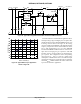
Figure 23. Voltage Inverting Demoboard Layout
Figure 24. Efficiency vs. Output Current for the
Voltage Inverting Demo Board at V
in
= +5 V,
V
out
= −12 V, T
A
= 255C
OUTPUT LOAD (mA
dc
)
8040200
36
38
40
44
46
48
50
52
EFFICIENCY (%)
60 100
42