
Datasheet


NCP3063, NCP3063B, NCV3063
http://onsemi.com
10
Figure 16. Typical Buck Application Schematic
J204
GND
1
J203
1
C203
2.2 nF
C202
C205
C206
C201
R202
U201
NCP3063
5
36
4
8
7
1
2
COMP
TCAP
GND
N.C. SWC
SWE
R203
R201
0R15
D201
1N5819
J202
GND
1
J201
1
L201
+V
IN
= +12 V
0.1 mF
2K4 ±1%
3K9 ±1%
220 mF / 50 V
+
0.1 mF
470 mF / 25 V
+
+V
OUT
= +3.3 V / 800 mA
V
CC
I
PK
47 mH
Value of Components
Name Value
L201
47 mH, I
sat
> 1.5 A
D201 1 A, 40 V Schottky Rectifier
C202
220 mF, 50 V, Low ESR
C205
470 mF, 25 V, Low ESR
C203 2.2 nF Ceramic Capacitor
Name Value
R201
150 mW, 0.5 W
R202
2.40 kW
R203
3.90 kW
C201 100 nF Ceramic Capacitor
C202 100 nF Ceramic Capacitor
Test Results
Test Condition Results
Line Regulation V
in
= 9 V to 12 V, I
o
= 800 mA 8 mV
Load Regulation V
in
= 12 V, I
o
= 80 mA to 800 mA 9 mV
Output Ripple V
in
= 12 V, I
o
= 40 mA to 800 mA ≤ 85 mV
pp
Efficiency V
in
= 12 V, I
o
= 400 mA to 800 mA > 73%
Short Circuit Current
V
in
= 12 V, R
load
= 0.15 W
1.25 A
Figure 17. Buck Demoboard Layout
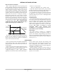
Figure 18. Efficiency vs. Output Current for the Buck
Demo Board at V
in
= 12 V, V
out
= 3.3 V, T
A
= 255C
OUTPUT LOAD (Adc)
0.1 0.2 0.3 0.4 0.5 0.6 0.7 0.8 0.9 1.0
EFFICIENCY (%)
76
74
72
70
68
66
64