
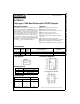
Data Sheet


3 www.fairchildsemi.com
NC7WZ125
Noise Characteristics
Note 4: Parameter guaranteed by design.
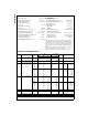
AC Electrical Characteristics
Note 5: Parameter guaranteed by design. t
OSLH
= |t
PLHmax
− t
PLHmin
|; t
OSHL
= |t
PHLmax
− t
PHLmin
|.
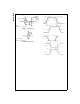
Note 6: C
PD
is defined as the value of the internal equivalent capacitance which is derived from dynamic operating current consumption (I
CCD
) at no output
loading and operating at 50% duty cycle. (See Figure 2.) C
PD
is related to I
CCD
dynamic operating current by the expression:
I
CCD
= (C
PD
)(V
CC
)(f
IN
) + (I
CC
static).
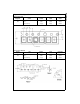
Symbol Parameter
V
CC
T
A
= + 25°C
Units Conditions
(V) Typ Max
V
OLP
(Note 4) Quiet Output Maximum Dynamic V
OL
5.0 1.0 V C
L
= 50 pF
V
OLV
(Note 4) Quiet Output Minimum Dynamic V
OL
5.0 1.0 V C
L
= 50 pF
V
OHV
(Note 4) Quiet Output Minimum Dynamic V
OH
5.0 4.0 V C
L
= 50 pF
V
IHD
(Note 4) Minimum HIGH Level Dynamic Input Voltage 5.0 3.5 V C
L
= 50 pF
V
ILD
(Note 4) Maximum LOW Level Dynamic Input Voltage 5.0 1.5 V C
L
= 50 pF
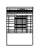
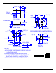
Symbol Parameter
V
CC
T
A
= +25°CT
A
= −40°C to +85°C
Units Conditions
Figure
(V) Min Typ Max Min Max Number
t
PLH
, Propagation Delay 1.8 ± 0.15 2.0 12.0 2.0 13.0
ns
C
L
= 15 pF
Figures
1, 3
t
PHL
A
N
to Y
N
2.5 ± 0.2 1.0 7.5 1.0 8.0 R
D
= 1 MΩ
3.3 ± 0.3 0.8 5.2 0.8 5.5 S1= Open
5.0 ± 0.5 0.5 4.5 0.5 4.8
t
PLH,
Propagation Delay 3.3 ± 0.3 1.2 5.7 1.2 6.0
ns
C
L
= 50 pF
Figures
1, 3
t
PHL
A
N
to Y
N
5.0 ± 0.5 0.8 5.0 0.8 5.3 R
D
= 500Ω
S1= Open
t
OSLH
, Output to Output Skew 3.3 ± 0.3 1.0 1.0
ns
C
L
= 50 pF
Figures
1, 3
t
OSHL
(Note 5) 5.0 ± 0.5 0.8 0.8 R
D
= 500Ω
S1= Open
t
PZL
, Output Enable Time 1.8 ± 0.15 3.0 14.0 3.0 15.0
ns
C
L
= 50 pF
t
PZH
2.5 ± 0.2 1.8 8.5 1.8 9.0 R
D
, R
U
= 500 Ω
Figures
1, 3
3.3 ± 0.3 1.2 6.2 1.2 6.5 S1 = GND for t
PZH
5.5 ± 0.5 0.8 5.5 0.8 5.8 S1 = V
I
for t
PZL
V
I
= 2 x V
CC
t
PLZ
, Output Disable Time 1.8 ± 0.15 2.5 12.0 2.5 13.0
ns
C
L
= 50 pF
Figures
1, 3
t
PHZ
2.5 ± 0.2 1.5 8.0 1.5 8.5 R
D
, R
U
= 500 Ω
3.3 ± 0.3 0.8 5.7 0.8 6.0 S1 = GND for t
PZH
5.0 ± 0.5 0.3 4.7 0.3 5.0 S1 = V
I
for t
PZL
V
I
= 2 x V
CC
C
IN
Input Capacitance 0 2.5
pF
C
OUT
Output Capacitance 5.0 4
C
PD
Power Dissipation Capacitance 3.3 10
pF (Note 6) Figure 2
5.0 12