
Data Sheet

www.fairchildsemi.com 2
NC7WZ125
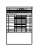
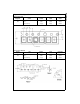
Absolute Maximum Ratings(Note 1) Recommended Operating
Conditions
(Note 3)
Note 1: Absolute maximum ratings are DC values beyond which the device
may be damaged or have its useful life impaired. The datasheet specifica-
tions should be met, without exception, to ensure that the system design is
reliable over its power supply, temperature, and output/input loading vari-
ables. Fairchild does not recommend operation outside datasheet specifi-
cations.
Note 2: The input and output negative voltage ratings may be exceeded if
the input and output diode current ratings are observed.
Note 3: Unused inputs must be held HIGH or LOW. They may not float.
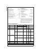
DC Electrical Characteristics
Supply Voltage (V
CC
) −0.5V to +7V
DC Input Voltage (V
IN
) (Note 2) −0.5V to +7V
DC Output Voltage (V
OUT
) −0.5V to +7V
DC Input Diode Current (I
IK
)
@V
IN
< 0V −50 mA
DC Output Diode Current (I
OK
)
@V
OUT
< 0V −50 mA
DC Output Source/Sink Current (I
OUT
) ± 50 mA
DC V
CC
/Ground Current (I
CC
/I
GND
) ± 100 mA
Storage Temperature Range (T
STG
) −65°C to +150°C
Junction Lead Temperature under Bias (T
J
) +150°C
Junction Lead Temperature (T
L
)
(Soldering, 10 seconds)
+260°C
Power Dissipation (P
D
) @ +85°C250 mW
Supply Voltage Operating (V
CC
) 1.65V to 5.5V
Supply Voltage Data Retention (V
CC
) 1.5V to 5.5V
Input Voltage (V
IN
) 0V to 5.5V
Output Voltage (V
OUT
)
Active State 0V to V
CC
3-STATE 0V to 5.5V
Operating Temperature (T
A
) −40°C to +85°C
Input Rise and Fall Time (t
r
, t
f
)
V
CC
@ 1.8V, 0.15V, 2.5V ± 0.2V 0 ns/V to 20 ns/V
V
CC
@ 3.3V ± 0.3V 0 ns/V to 10 ns/V
V
CC
@ 5.0V ± 0.5V 0 ns/V to 5 ns/V
Thermal Resistance (
θ
JA
)250°C/W
Symbol Parameter
V
CC
T
A
= +25°CT
A
= −40°C to +85°C
Units Conditions
(V) Min Typ Max Min Max
V
IH
HIGH Level Input Voltage 1.65 to 1.95 0.75 V
CC
0.75 V
CC
V
2.3 to 5.5 0.7 V
CC
0.7 V
CC
V
IL
LOW Level Input Voltage 1.65 to 1.95 0.25 V
CC
0.25 V
CC
V
2.3 to 5.5 0.3 V
CC
0.3 V
CC
V
OH
HIGH Level Output Voltage 1.65 1.55 1.65 1.55
V
2.3 2.2 2.3 2.2 V
IN
= V
IH
I
OH
= −100 µA
3.0 2.9 3.0 2.9 or V
IL
4.5 4.4 4.5 4.4
1.65 1.29 1.52 1.29
V
I
OH
= −4 mA
2.3 1.9 2.15 1.9 V
IN
= V
IH
I
OH
= −8 mA
3.0 2.4 2.80 2.4 or V
IL
I
OH
= −16 mA
3.0 2.3 2.68 2.3 I
OH
= −24 mA
4.5 3.8 4.20 3.8 I
OH
= −32 mA
V
OL
LOW Level Output Voltage 1.65 0.0 0.10 0.10
V
2.3 0.0 0.10 0.10 V
IN
= V
IH
I
OL
= 100 µA
3.0 0.0 0.10 0.10 or V
IL
4.5 0.0 0.10 0.10
1.65 0.08 0.24 0.24
V
I
OL
= 4 mA
2.3 0.10 0.3 0.3 I
OL
= 8 mA
3.0 0.15 0.4 0.4 I
OL
= 16 mA
3.0 0.22 0.55 0.55 I
OL
= 24 mA
4.5 0.22 0.55 0.55 I
OL
= 32 mA
I
IN
Input Leakage Current 0 to 5.5 ±0.1 ±1 µAV
IN
= 5.5V, GND
I
OZ
3-STATE Output Leakage 1.65 to 5.5 ±0.5 ±5 µAV
IN
= V
IH
or V
IL
0 ≤ V
OUT
≤ 5.5V
I
OFF
Power Off Leakage Current 0.0 1 10 µAV
IN
or V
OUT
= 5.5V
I
CC
Quiescent Supply Current 1.65 to 5.5 1 10 µAV
IN
= 5.5V, GND