
Data Sheet
© 2000 Fairchild Semiconductor Corporation www.fairchildsemi.com
NC7WZ07 • Rev. 1.0.7 3
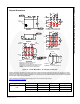
NC7WZ07 — TinyLogic
®
UHS Dual Buffer (Open-Drain Outputs)
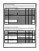
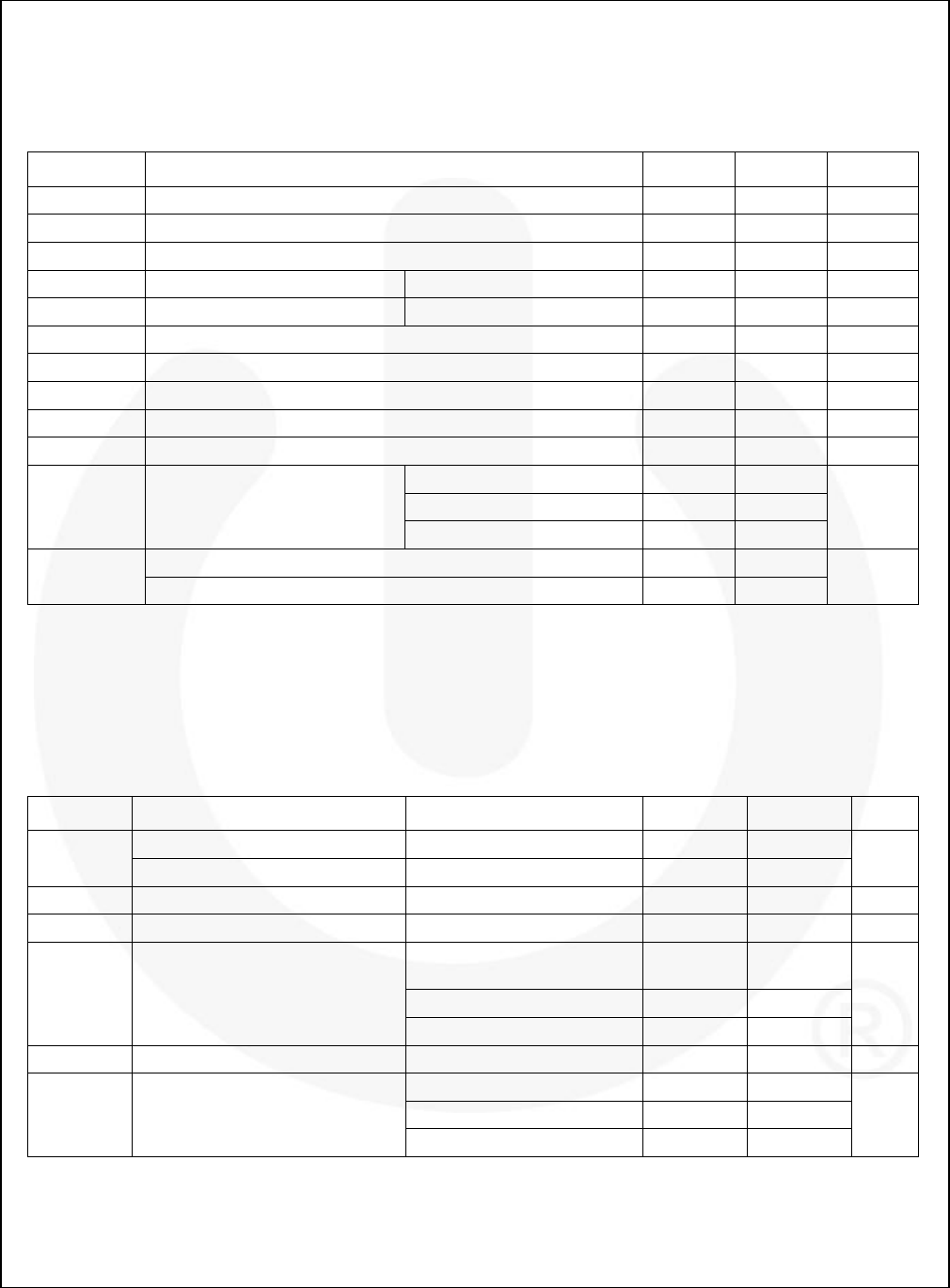
Absolute Maximum Ratings
Stresses exceeding the absolute maximum ratings may damage the device. The device may not function or be
operable above the recommended operating conditions and stressing the parts to these levels is not recommended.
In addition, extended exposure to stresses above the recommended operating conditions may affect device reliability.
The absolute maximum ratings are stress ratings only.
Symbol
Parameter
Min.
Max.
Unit
V
CC
Supply Voltage
-0.5
7.0
V
V
IN
DC Input Voltage
-0.5
7.0
V
V
OUT
DC Output Voltage
-0.5
7.0
V
I
IK
DC Input Diode Current
V
IN
< -0.5 V
-50
mA
I
OK
DC Output Diode Current
V
OUT
< -0.5 V
-50
mA
I
OUT
DC Output Current
±50
mA
I
CC
or I
GND
DC V
CC
or Ground Current
±100
mA
T
STG
Storage Temperature Range
-65
+150
°C
T
J
Junction Temperature Under Bias
+150
°C
T
L
Junction Lead Temperature (Soldering, 10 Seconds)
+260
°C
P
D
Power Dissipation at +85°C
SC70-6
150
mW
MicroPak™-6
130
MicroPak2™-6
120
ESD
Human Body Model, JEDEC:JESD22-A114
4000
V
Charge Device Model, JEDEC:JESD22-C101
2000
Recommended Operating Conditions
The Recommended Operating Conditions table defines the conditions for actual device operation. Recommended
operating conditions are specified to ensure optimal performance to the datasheet specifications. Fairchild does not
recommend exceeding them or designing to Absolute Maximum Ratings.
Symbol
Parameter
Conditions
Min.
Max.
Unit
V
CC
Supply Voltage Operating
1.65
5.50
V
Supply Voltage Data Retention
1.5
5.5
V
IN
Input Voltage
0
5.5
V
V
OUT
Output Voltage
0
5.5
V
t
r
, t
f
Input Rise and Fall Times
V
CC
at 1.8 V, ±0.15 V,
2.5 V ± 0.2 V
0
20
ns/V
V
CC
at 3.3 V ±0.3 V
0
10
V
CC
at 5.0 V ±0.5 V
0
5
T
A
Operating Temperature
-40
+85
°C
JA
Thermal Resistance
SC70-6
425
°C/W
MicroPak™-6
500
MicroPak2™-6
560
Note:
4. Unused inputs must be held HIGH or LOW. They may not float.