
Data Sheet


MOCD207M, MOCD208M, MOCD211M, MOCD213M, MOCD217M
www.onsemi.com
3
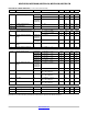
ABSOLUTE MAXIMUM RATINGS (T
A
= 25°C unless otherwise noted)
Symbol
Rating Value Unit
TOTAL DEVICE
T
STG
Storage Temperature −40 to +125 °C
T
A
Ambient Operating Temperature −40 to +100 °C
T
J
Junction Temperature −40 to +125 °C
T
SOL
Lead Solder Temperature 260 for 10 seconds °C
P
D
Total Device Power Dissipation @ T
A
= 25°C 240 mW
Derate Above 25°C 2.94 mW/°C
EMITTER
I
F
Continuous Forward Current 60 mA
I
F
(pk)
Forward Current – Peak (PW = 100 ms, 120 pps)
1.0 A
V
R
Reverse Voltage 6.0 V
P
D
LED Power Dissipation @ T
A
= 25°C 90 mW
Derate Above 25°C 0.8 mW/°C
DETECTOR
I
C
Continuous Collector Current 150 mA
V
CEO
Collector−Emitter Voltage
− MOCD207M, MOCD208M
70 V
− MOCD211M, MOCD213M, MOCD217M 30 V
V
ECO
Emitter−Collector Voltage 7 V
P
D
Detector Power Dissipation @ T
A
= 25°C 150 mW
Derate Above 25°C 1.76 mW/°C
Stresses exceeding those listed in the Maximum Ratings table may damage the device. If any of these limits are exceeded, device functionality
should not be assumed, damage may occur and reliability may be affected.