
Data Sheet


FFB2222A / FMB2222A / MMPQ2222A — NPN Multi-Chip General-Purpose Amplifier
© 1998 Fairchild Semiconductor Corporation www.fairchildsemi.com
FFB2222A / FMB2222A / MMPQ2222A Rev. 1.4 2
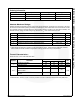
Ordering Information
Absolute Maximum Ratings
(1)
Stresses exceeding the absolute maximum ratings may damage the device. The device may not function or be opera-
ble above the recommended operating conditions and stressing the parts to these levels is not recommended. In addi-
tion, extended exposure to stresses above the recommended operating conditions may affect device reliability. The
absolute maximum ratings are stress ratings only. Values are at T
A
= 25°C unless otherwise noted.
Note:
1. These ratings are based on a maximum junction temperature of 150°C. These are steady-state limits. Fairchild
Semiconductor should be consulted on applications involving pulsed or low-duty cycle operations.
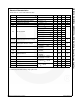
Thermal Characteristics
(2)
Values are at T
A
= 25°C unless otherwise noted.
Note:
2. PCB size: FR-4, 76 mm x 114 mm x 1.57 mm (3.0 inch x 4.5 inch x 0.062 inch) with minimum land pattern size.
Part Number
Top Mark
Package Packing Method
FFB2222A .1P SC70 6L Tape and Reel
FMB2222A .1P SSOT 6L Tape and Reel
MMPQ2222A MMPQ2222A SOIC 16L Tape and Reel
Symbol Parameter Value Unit
V
CEO
Collector-Emitter Voltage 45 V
V
CBO
Collector-Base Voltage 75 V
V
EBO
Emitter-Base Voltage 5.0 V
I
C
Collector Current - Continuous 500 mA
T
J
, T
STG
Operating and Storage Junction Temperature Range -55 to +150 °C
Symbol Parameter
Max.
Unit
FFB2222A FMB2222A MMPQ2222A
P
D
Total Device Dissipation 300 700 1,000 mW
Derate Above 25°C 2.4 5.6 8.0 mW/°C
R
θJA
Thermal Resistance, Junction-to-Ambient 415 180
°C/W
Thermal Resistance, Junction-to-Ambient,
Effective 4 Dies
125
Thermal Resistance, Junction-to-Ambient,
Each Die
240