
Data Sheet


© 1983 Fairchild Semiconductor Corporation www.fairchildsemi.com
MM74HC595 • Rev. 1.0.2 6
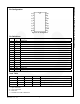
MM74HC595 — 8-Bit Shift Register with Output Latches
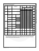
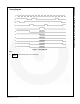
AC Electrical Characteristics
V
CC
= 5V, T
A
= 25°C, t
r
= t
f
= 6ns.
Symbol Parameter Conditions Typ. Guaranteed Limit Units
f
MAX
Maximum Operating Frequency of SCK 50 30 MHz
Maximum Propagation Delay, SCK to Q’
H
12 20
t
PHL
,t
PLH
Maximum Propagation Delay, RCK to Q
A
thru Q’
H
C
L
=45pF
18 30
ns
t
PZH
,t
PZL
Maximum Output Enable Time from G to
Q
A
thru Q’
H
R
L
=1kΩ, C
L
=45pF
17 28 ns
t
PHZ
,t
PLZ
Maximum Output Disable Time from G to
Q
A
thru Q’
H
R
L
=1kΩ, C
L
=45pF
15 25 ns
Minimum Setup Time from SER to SCK 20 ns
Minimum Setup Time from SCLR to SCK 20 ns
t
S
Minimum Setup Time from SER to
RCK
(4)
40 ns
t
H
Minimum Hold Time from SER to SCK 0 ns
t
W
Minimum Pulse Width of SCK or RCK 16 ns
Note:
4. This setup time ensures the register will see stable data from the shift-register outputs. The clocks may be
connected together in which case the storage register state will be one clock pulse behind the shift register.