
Data Sheet


© 1983 Fairchild Semiconductor Corporation www.fairchildsemi.com
MM74HC595 • Rev. 1.0.2 8
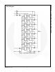
MM74HC595 — 8-Bit Shift Register with Output Latches
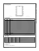
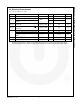
Electrical Characteristics
V
CC
= 2.0−6.0V, C
L
= 50pF, t
r
= t
f
=6ns unless otherwise specified.
T
A
=25°C
T
A
=-40 to
85°C
T
A
=-55
to 125°C
Symbol Parameter Conditions V
CC
Typ. Guaranteed Limits
Units
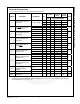
2.0V 100 125 150
4.5V 20 25 30
t
S
Minimum Setup Time from
SER to SCK
R
L
=1kΩ, C
L
=50pF
6.0V 17 21 25
ns
2.0V 50 63 75
4.5V 10 13 15
t
R
Minimum Removal Time
from SCLR to SCK
6.0V 9 11 13
ns
2.0V 100 125 150
4.5V 20 25 30
t
S
Minimum Setup Time from
SCK to RCK
6.0V 17 21 26
ns
2.0V 5 5 5
4.5V 5 5 5
t
H
Minimum Hold Time from
SER to SCK
6.0V 5 5 5
ns
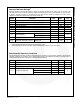
2.0V 30 80 100 120
4.5V 9 16 20 24
t
W
Minimum Pulse Width of
SCK or SCLR
6.0V 8 14 18 22
ns
2.0V 1000 1000 1000
4.5V 500 500 500
t
R
,t
F
Maximum Input Rise and
Fall Time, Clock
6.0V 400 400 400
ns
2.0V 25 60 75 90
4.5V 7 12 15 18
Maximum Output Rise and
Fall Time Q
A
-Q
H
6.0V 6 10 13 15
ns
2.0V 75 95 110
4.5V 15 19 22
t
THL
,t
TLH
Maximum Output Rise and
Fall Time Q’
H
6.0V
13 16
19
ns
G=V
CC
90
C
PD
Power Dissipation
Capacitance, Outputs
Enabled
(5)
G=GND
150
pF
C
IN
Maximum Input Capacitance 5 10 10 10 pF
C
OUT
Maximum Output
Capacitance
15 20 20 20 pF
Note:
5. C
PD
determines the no load dynamic power consumption, P
D
= C
PD
V
CC
2
f + I
CC
V
CC
, and the no load dynamic
current consumption, I
S
= C
PD
V
CC
f + I
CC
.