
Data Sheet

MM74HC574
www.onsemi.com
2
ORDERING CODE
Order Number Package Number Package Description
MM74HC574WM M20B 20−Lead Small Outline Integrated Circuit (SOIC), JEDEC MS−013, 0.300″ Wide
MM74HC574SJ M20D 20−Lead Small Outline Package (SOP), EIAJ TYPE II, 5.3 mm Wide
MM74HC574MTC MTC20 20−Lead Thin Shrink Small Outline Package (TSSOP), JEDEC MO−153, 4.4 mm Wide
MM74HC574N N20A 20−Lead Plastic Dual−In−Line Package (PDIP), JEDEC MS−001, 0.300″ Wide
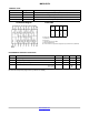
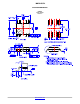
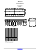
Connection Diagram
Pin Assignments for DIP, SOIC, SOP and TSSOP
Top View
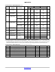
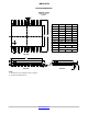
Truth Table
Output Clock Data Output
Control
L
L
L
H
L
X
H
L
X
X
H
L
Z
↑
↑
Q
0
H = HIGH Level
L = LOW Level
X = Don’t Care
↑ = Transition from Low−to−HIGH
Z = High Impedance State
Q0 = The level of the output before steady state input conditions were established
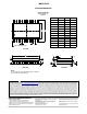
RECOMMENDED OPERATING CONDITIONS
Symbol Characteristic Min Typ Max Units
V
CC
Supply Voltage 2 6 V
V
IN
, V
OUT
DC Input or Output Voltage 0 V
CC
V
T
A
Operating Temperature Range −55 +125 °C
t
r
, t
f
Input Rise or Fall Times V
CC
= 2.0 V
V
CC
= 4.5 V
V
CC
= 6.0 V
1000
500
400
ns
Functional operation above the stresses listed in the Recommended Operating Ranges is not implied. Extended exposure to stresses beyond
the Recommended Operating Ranges limits may affect device reliability.