
Data Sheet

© Semiconductor Components Industries, LLC, 1983
November, 2017 − Rev. 2
1 Publication Order Number:
MM74HC574/D
MM74HC574
3-State Octal D-Type
Edge-Triggered Flip-Flop
The MM74HC574 high speed octal D−type flip−flops utilize
advanced silicon−gate P−well CMOS technology. They possess the
high noise immunity and low power consumption of standard CMOS
integrated circuits, as well as the ability to drive 15 LS−TTL loads.
Due to the large output drive capability and the 3−STATE feature,
these devices are ideally suited for interfacing with bus lines in a bus
organized system.
These devices are positive edge triggered flip−flops. Data at the D
inputs, meeting the set−up and hold time requirements, are transferred
to the Q outputs on positive going transitions of the CLOCK (CK)
input. When a high logic level is applied to the OUTPUT CONTROL
(OC) input, all outputs go to a high impedance state, regardless of
what signals are present at the other inputs and the state of the storage
elements.
The 74HC logic family is speed, function, and pinout compatible with
the standard 74LS logic family. All inputs are protected from damage
due to static discharge by internal diode clamps to V
CC
and ground.
Features
• Typical Propagation Delay: 18 ns
• Wide Operating Voltage Range: 2 V – 6 V
• Low Input Current: 1 mA Maximum
• Low Quiescent Current: 80 mA Maximum
• Compatible with Bus−oriented Systems
• Output Drive Capability: 15 LS−TTL Loads
MAXIMUM RATINGS (Note 1)
Rating
Symbol Value Unit
Supply Voltage V
CC
−0.5 to +
7.0 V
V
DC Input Voltage V
IN
−1.5 to V
CC
+ 1.5 V
V
DC Output Voltage V
OUT
−0.5 to V
CC
+ 0.5 V
V
Clamp Diode Current I
IK
, I
OK
±20 mA
DC Output Current, per pin I
OUT
±35 mA
DC V
CC
or GND Current, per pin I
CC
±70 mA
Storage Temperature Range T
STG
−65 to
+150
°C
Power Dissipation (Note 2)
S.O. Package only
P
D
600
500
mW
Lead Temperature (Soldering 10 s) T
L
260 °C
Stresses exceeding those listed in the Maximum Ratings table may damage the
device. If any of these limits are exceeded, device functionality should not be
assumed, damage may occur and reliability may be affected.
1. Unless otherwise specified all voltages are referenced to ground.
2. Power Dissipation temperature derating — plastic “N” package: −
12 mW/°C from 65°C to 85°C.
www.onsemi.com
See detailed ordering and shipping information in the package
dimensions section on page 2 of this data sheet.
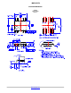
ORDERING INFORMATION
TSSOP20
MTC SUFFIX
CASE 948AQ
SOP20
SJ SUFFIX
CASE 565BG
PDIP20
N SUFFIX
CASE 646AC
SOIC20
WM SUFFIX
CASE 751BJ