
Data Sheet
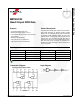


MM74HC02 — Quad 2-Input NOR Gate
© 1983 Fairchild Semiconductor Corporation www.fairchildsemi.com
MM74HC02 Rev. 1.4 2
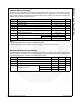
Absolute Maximum Ratings
(1)
Stresses exceeding the absolute maximum ratings may damage the device. The device may not function or be opera-
ble above the recommended operating conditions and stressing the parts to these levels is not recommended. In addi-
tion, extended exposure to stresses above the recommended operating conditions may affect device reliability. The
absolute maximum ratings are stress ratings only.
Notes:
1. Unless otherwise specified all voltages are referenced to ground.
2. Power dissipation temperature derating - plastic “N” package: -12 mW/°C from 65°C to 85°C.
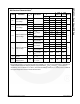
Recommended Operating Conditions
The Recommended Operating Conditions table defines the conditions for actual device operation. Recommended
operating conditions are specified to ensure optimal performance to the datasheet specifications. Fairchild does not
recommend exceeding them or designing to absolute maximum ratings.
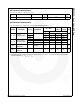
Symbol Parameter Value Unit
V
CC
Supply Voltage -0.5 to +7.0 V
V
IN
DC Input Voltage -1.5 to V
CC
+1.5 V
V
OUT
DC Output Voltage -0.5 to V
CC
+0.5 V
I
IK
, I
OK
Clamp Diode Current ±20 mA
I
OUT
DC Output Current, per pin ±25 mA
I
CC
DC V
CC
or GND Current, per pin
±50 mA
T
STG
Storage Temperature Range -65 to +150 °C
P
D
Power Dissipation
(2)
600
mW
S.O. Package only 500
T
L
Lead Temperature (Soldering 10 seconds) 260 °C
Symbol Parameter Min. Max. Unit
V
CC
Supply Voltage 2 6 V
V
IN
, V
OUT
DC Input or Output Voltage 0 V
CC
V
T
A
Operating Temperature Range -40 85 °C
t
r
, t
f
Input Rise or Fall Times
V
CC
= 2.0 V 1000
nsV
CC
= 4.5 V 500
V
CC
= 6.0 V 400