
Data Sheet

MJE350G
www.onsemi.com
2
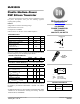
V
, TEMPERATURE COEFFICIENTS (mV/ C)°θ
I
C
, COLLECTOR CURRENT (mA)
h
FE
, DC CURRENT GAIN
200
7.0 205.0
50
30
10
10 50 10030
25°C
T
J
= 150°C
-55°C
Figure 1. DC Current Gain
100
20
70
200 50030070
V
CE
= 2.0 V
V
CC
= 10 V
Figure 2. “On” Voltages
1.0
I
C
, COLLECTOR CURRENT (mA)
0.8
0.2
0
T
J
= 25°C
V, VOLTAGE (VOLTS)
V
BE(sat)
@ I
C
/I
B
= 10
V
BE
@ V
CE
= 10 V0.6
0.4
V
CE(sat)
7.0 205.0 10 50 10030 200 50030070
I
C
/I
B
= 10
I
C
/I
B
= 5.0
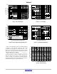
1000
V
CE
, COLLECTOR-EMITTER VOLTAGE (VOLTS)
70
300
10
50
BONDING WIRE LIMITED
THERMALLY LIMITED @ T
C
= 25°C
SECOND BREAKDOWN LIMITED
Figure 3. Active−Region Safe Operating Area
1.0ms
dc
700
2001005020
T
J
= 150°C
I
C
, COLLECTOR CURRENT (mA)
100
300
500
30
100ms
40030 70
200
20
500ms
+1.2
I
C
, COLLECTOR CURRENT (mA)
70
Figure 4. Temperature Coefficients
5030105.0 5007.0 20
+0.8
+0.4
0
-0.4
-0.8
-1.2
-1.6
-2.0
-2.4
-2.8
100 200 300
*APPLIES FOR I
C
/I
B
< h
FE/4
*q
VC
for V
CE(sat)
q
VB
for V
BE
+100°C to +150°C
+25°C to +100°C
-55°C to +25°C
+25°C to +150°C
-55°C to +25°C
There are two limitations on the power handling ability of
a transistor: average junction temperature and second
breakdown. Safe operating area curves indicate I
C
− V
CE
limits of the transistor that must be observed for reliable
operation; i.e., the transistor must not be subjected to greater
dissipation than the curves indicate.
The data of Figure 3 is based on T
J(pk)
= 150_C; T
C
is
variable depending on conditions. Second breakdown pulse
limits are valid for duty cycles to 10% provided T
J(pk)
≤ 150_C. At high case temperatures, thermal limitations
will reduce the power that can be handled to values less than
the limitations imposed by second breakdown.
20
T
C
, CASE TEMPERATURE (°C)
Figure 5. Power Derating
10080400 16020 60
16
12
8.0
4.0
0
120 140
P
D
, POWER DISSIPATION (WATTS)