
Data Sheet
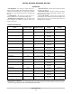


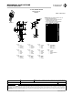


DPAK (SINGLE GAUGE)
CASE 369C
ISSUE F
DATE 21 JUL 2015
SCALE 1:1
STYLE 1:
PIN 1. BASE
2. COLLECTOR
3. EMITTER
4. COLLECTOR
STYLE 2:
PIN 1. GATE
2. DRAIN
3. SOURCE
4. DRAIN
STYLE 3:
PIN 1. ANODE
2. CATHODE
3. ANODE
4. CATHODE
STYLE 4:
PIN 1. CATHODE
2. ANODE
3. GATE
4. ANODE
STYLE 5:
PIN 1. GATE
2. ANODE
3. CATHODE
4. ANODE
STYLE 6:
PIN 1. MT1
2. MT2
3. GATE
4. MT2
STYLE 7:
PIN 1. GATE
2. COLLECTOR
3. EMITTER
4. COLLECTOR
1
2
3
4
STYLE 8:
PIN 1. N/C
2. CATHODE
3. ANODE
4. CATHODE
STYLE 9:
PIN 1. ANODE
2. CATHODE
3. RESISTOR ADJUST
4. CATHODE
STYLE 10:
PIN 1. CATHODE
2. ANODE
3. CATHODE
4. ANODE
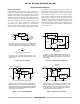
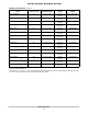
b
D
E
b3
L3
L4
b2
M
0.005 (0.13) C
c2
A
c
C
Z
DIM MIN MAX MIN MAX
MILLIMETERSINCHES
D 0.235 0.245 5.97 6.22
E 0.250 0.265 6.35 6.73
A 0.086 0.094 2.18 2.38
b 0.025 0.035 0.63 0.89
c2 0.018 0.024 0.46 0.61
b2 0.028 0.045 0.72 1.14
c 0.018 0.024 0.46 0.61
e 0.090 BSC 2.29 BSC
b3 0.180 0.215 4.57 5.46
L4 −−− 0.040 −−− 1.01
L 0.055 0.070 1.40 1.78
L3 0.035 0.050 0.89 1.27
Z 0.155 −−− 3.93 −−−
NOTES:
1. DIMENSIONING AND TOLERANCING PER ASME
Y14.5M, 1994.
2. CONTROLLING DIMENSION: INCHES.
3. THERMAL PAD CONTOUR OPTIONAL WITHIN DI-
MENSIONS b3, L3 and Z.
4. DIMENSIONS D AND E DO NOT INCLUDE MOLD
FLASH, PROTRUSIONS, OR BURRS. MOLD
FLASH, PROTRUSIONS, OR GATE BURRS SHALL
NOT EXCEED 0.006 INCHES PER SIDE.
5. DIMENSIONS D AND E ARE DETERMINED AT THE
OUTERMOST EXTREMES OF THE PLASTIC BODY.
6. DATUMS A AND B ARE DETERMINED AT DATUM
PLANE H.
7. OPTIONAL MOLD FEATURE.
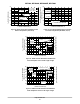
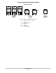
12 3
4
XXXXXX = Device Code
A = Assembly Location
L = Wafer Lot
Y = Year
WW = Work Week
G = Pb−Free Package
AYWW
XXX
XXXXXG
XXXXXXG
ALYWW
DiscreteIC
5.80
0.228
2.58
0.102
1.60
0.063
6.20
0.244
3.00
0.118
6.17
0.243
ǒ
mm
inches
Ǔ
SCALE 3:1
GENERIC
MARKING DIAGRAM*
*This information is generic. Please refer
to device data sheet for actual part
marking.
*For additional information on our Pb−Free strategy and soldering
details, please download the ON Semiconductor Soldering and
Mounting Techniques Reference Manual, SOLDERRM/D.
SOLDERING FOOTPRINT*
H 0.370 0.410 9.40 10.41
A1 0.000 0.005 0.00 0.13
L1 0.114 REF 2.90 REF
L2 0.020 BSC 0.51 BSC
A1
H
DETAIL A
SEATING
PLANE
A
B
C
L1
L
H
L2
GAUGE
PLANE
DETAIL A
ROTATED 90 CW5
e
BOTTOM VIEW
Z
BOTTOM VIEW
SIDE VIEW
TOP VIEW
ALTERNATE
CONSTRUCTIONS
NOTE 7
Z
MECHANICAL CASE OUTLINE
PACKAGE DIMENSIONS
ON Semiconductor and are trademarks of Semiconductor Components Industries, LLC dba ON Semiconductor or its subsidiaries in the United States and/or other countries.
ON Semiconductor reserves the right to make changes without further notice to any products herein. ON Semiconductor makes no warranty, representation or guarantee regarding
the suitability of its products for any particular purpose, nor does ON Semiconductor assume any liability arising out of the application or use of any product or circuit, and specifically
disclaims any and all liability, including without limitation special, consequential or incidental damages. ON Semiconductor does not convey any license under its patent rights nor the
rights of others.
98AON10527D
DOCUMENT NUMBER:
DESCRIPTION:
Electronic versions are uncontrolled except when accessed directly from the Document Repository.
Printed versions are uncontrolled except when stamped “CONTROLLED COPY” in red.
PAGE 1 OF 1
DPAK (SINGLE GAUGE)
© Semiconductor Components Industries, LLC, 2018
www.onsemi.com