
Datasheet


MC34071,2,4,A MC33071,2,4,A, NCV33072,4,A
http://onsemi.com
5
AC ELECTRICAL CHARACTERISTICS (V
CC
= +15 V, V
EE
= −15 V, R
L
= connected to ground. T
A
= +25°C, unless otherwise noted.)
A Suffix Non−Suffix
Characteristics Symbol Min Typ Max Min Typ Max Unit
Slew Rate (V
in
= −10 V to +10 V, R
L
= 2.0 kW, C
L
= 500 pF)
A
V
= +1.0
A
V
= −1.0
SR
8.0
−
10
13
−
−
8.0
−
10
13
−
−
V/ms
Setting Time (10 V Step, A
V
= −1.0)
To 0.1% (+1/2 LSB of 9−Bits)
To 0.01% (+1/2 LSB of 12−Bits)
t
s
−
−
1.1
2.2
−
−
−
−
1.1
2.2
−
−
ms
Gain Bandwidth Product (f = 100 kHz) GBW 3.5 4.5 − 3.5 4.5 − MHz
Power Bandwidth
A
V
= +1.0, R
L
= 2.0 kW, V
O
= 20 V
pp
, THD = 5.0%
BW − 160 − − 160 − kHz
Phase margin
R
L
= 2.0 kW
R
L
= 2.0 kW, C
L
= 300 pF
f
m
−
−
60
40
−
−
−
−
60
40
−
−
Deg
Gain Margin
R
L
= 2.0 kW
R
L
= 2.0 kW, C
L
= 300 pF
A
m
−
−
12
4.0
−
−
−
−
12
4.0
−
−
dB
Equivalent Input Noise Voltage
R
S
= 100 W, f = 1.0 kHz
e
n
− 32 − − 32 −
nV/ H
z
√
Equivalent Input Noise Current
f = 1.0 kHz
i
n
− 0.22 − − 0.22 −
pA/ H
z
√
Differential Input Resistance
V
CM
= 0 V
R
in
− 150 − − 150 −
MW
Differential Input Capacitance
V
CM
= 0 V
C
in
− 2.5 − − 2.5 − pF
Total Harmonic Distortion
A
V
= +10, R
L
= 2.0 kW, 2.0 V
pp
≤ V
O
≤ 20 V
pp
, f = 10 kHz
THD − 0.02 − − 0.02 − %
Channel Separation (f = 10 kHz) − − 120 − − 120 − dB
Open Loop Output Impedance (f = 1.0 MHz) |Z
O
| − 30 − − 30 − W
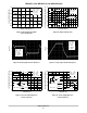
Figure 2. Power Supply Configurations Figure 3. Offset Null Circuit
Single Supply Split Supplies
1
2
3
4
V
CC
V
EE
V
CC
V
CC
V
EE
V
EE
1
2
3
4
3.0 V to 44 V V
CC
+|V
EE
|≤44 V
Offset nulling range is approximately ±80 mV with a 10 k
potentiometer (MC33071, MC34071 only).
V
CC
V
EE
1
2
3
4
5
6
7
10 k
+
-