
Datasheet
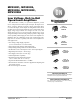

MC33201, MC33202, MC33204, NCV33202, NCV33204
http://onsemi.com
3
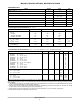
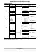
MAXIMUM RATINGS
Rating Symbol Value Unit
Supply Voltage (V
CC
to V
EE
) V
S
+13 V
Input Differential Voltage Range V
IDR
Note 1 V
Common Mode Input Voltage Range (Note 2) V
CM
V
CC
+ 0.5 V to
V
EE
− 0.5 V
V
Output Short Circuit Duration t
s
Note 3 sec
Maximum Junction Temperature T
J
+150 °C
Storage Temperature T
stg
− 65 to +150 °C
Maximum Power Dissipation P
D
Note 3 mW
DC ELECTRICAL CHARACTERISTICS (T
A
= 25°C)
Characteristic V
CC
= 2.0 V V
CC
= 3.3 V V
CC
= 5.0 V Unit
Input Offset Voltage
V
IO
(max)
MC33201
MC33202, NCV33202
MC33204, NCV33204
± 8.0
±10
±12
± 8.0
±10
±12
± 6.0
± 8.0
±10
mV
Output Voltage Swing
V
OH
(R
L
= 10 kW)
V
OL
(R
L
= 10 kW)
1.9
0.10
3.15
0.15
4.85
0.15
V
min
V
max
Power Supply Current
per Amplifier (I
D
)
1.125 1.125 1.125
mA
Specifications at V
CC
= 3.3 V are guaranteed by the 2.0 V and 5.0 V tests. V
EE
= GND.
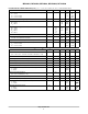
DC ELECTRICAL CHARACTERISTICS (V
CC
= + 5.0 V, V
EE
= Ground, T
A
= 25°C, unless otherwise noted.)
Characteristic Figure Symbol Min Typ Max Unit
Input Offset Voltage (V
CM
0 V to 0.5 V, V
CM
1.0 V to 5.0 V)
MC33201: T
A
= + 25°C
MC33201: T
A
= − 40° to +105°C
MC33201V: T
A
= − 55° to +125°C
MC33202: T
A
= + 25°C
MC33202: T
A
= − 40° to +105°C
MC33202V: T
A
= − 55° to +125°C
NCV33202V: T
A
= − 55° to +125°C (Note 4)
MC33204: T
A
= + 25°C
MC33204: T
A
= − 40° to +105°C
MC33204V: T
A
= − 55° to +125°C
NCV33204: T
A
= − 55° to +125°C
3 ⎮V
IO
⎮
−
−
−
−
−
−
−
−
−
−
−
−
−
−
−
−
−
−
−
−
−
−
6.0
9.0
13
8.0
11
14
14
10
13
17
17
mV
Input Offset Voltage Temperature Coefficient (R
S
= 50 W)
T
A
= − 40° to +105°C
T
A
= − 55° to +125°C
4
DV
IO
/DT
−
−
2.0
2.0
−
−
mV/°C
Input Bias Current (V
CM
= 0 V to 0.5 V, V
CM
= 1.0 V to 5.0 V)
T
A
= + 25°C
T
A
= − 40° to +105°C
T
A
= − 55° to +125°C
5, 6 ⎮I
IB
⎮
−
−
−
80
100
−
200
250
500
nA
Stresses exceeding Maximum Ratings may damage the device. Maximum Ratings are stress ratings only. Functional operation above the
Recommended Operating Conditions is not implied. Extended exposure to stresses above the Recommended Operating Conditions may affect
device reliability.
1. The differential input voltage of each amplifier is limited by two internal parallel back−to−back diodes. For additional differential input voltage
range, use current limiting resistors in series with the input pins.
2. The input common mode voltage range is limited by internal diodes connected from the inputs to both supply rails. Therefore, the voltage
on either input must not exceed either supply rail by more than 500 mV.
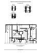
3. Power dissipation must be considered to ensure maximum junction temperature (T
J
) is not exceeded. (See Figure 2)
4. NCV33202 and NCV33204 are qualified for automotive use.