
Datasheet


MC34063A, MC33063A, NCV33063A
http://onsemi.com
4
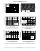
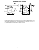
t
on
V
CC
= 5.0 V
Pin 7 = V
CC
Pin 5 = GND
T
A
= 25°C
t
off
Figure 2. Output Switch On−Off Time versus
Oscillator Timing Capacitor
Figure 3. Timing Capacitor Waveform
0.01 0.02 0.05 0.1 0.2 0.5 1.0 2.0 5.0 10
C
T
, OSCILLATOR TIMING CAPACITOR (nF)
, OUTPUT SWITCH ON-OFF TIME ( s)
on−off
μ
t
10 ms/DIV
, OSCILLATOR VOLTAGE (V)
OSC
200 mV/DIV
V
V
CC
= 5.0 V
Pin 7 = V
CC
Pin 2 = GND
Pins 1, 5, 8 = Open
C
T
= 1.0 nF
T
A
= 25°C
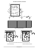
1000
500
200
100
50
20
10
5.0
2.0
1.0
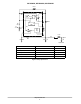
Figure 4. Emitter Follower Configuration Output
Saturation Voltage versus Emitter Current
Figure 5. Common Emitter Configuration Outpu
t
Switch Saturation Voltage versus
Collector Current
Figure 6. Current Limit Sense Voltage
versus Temperature
Figure 7. Standby Supply Current versus
Supply Voltage
0 0.2 0.4 0.6 0.8 1.0 1.2 1.4 1.6
, SATURATION VOLTAGE (V)
CE(sat)
I
E
, EMITTER CURRENT (A)
V
V
CC
= 5.0 V
Pins 1, 7, 8 = V
CC
Pins 3, 5 = GND
T
A
= 25°C
(See Note 7)
, SATURATION VOLTAGE (V)
CE(sat)
0 0.2 0.4 0.6 0.8 1.0 1.2 1.4 1.6
I
C
, COLLECTOR CURRENT(A)
V
Darlington Connection
Forced b = 20
−55 −25 0 25 50 75 100 125
, CURRENT LIMIT SENSE VOLTAGE (V)
IPK(sense)
T
A
, AMBIENT TEMPERATURE (°C)
V
V
CC
= 5.0 V
I
chg
= I
dischg
0 5.0 10 15 20 25 30 35 40
, SUPPLY CURRENT (mA)
CC
V
CC
, SUPPLY VOLTAGE (V)
I
C
T
= 1.0 nF
Pin 7 = V
CC
Pin 2 = GND
1.8
1.7
1.6
1.5
1.4
1.3
1.2
1.1
1.0
1.1
0.9
0.8
0.7
0.6
0.5
0.4
0.3
0.2
0.1
0
400
380
360
340
320
300
280
260
240
220
200
3.6
3.2
2.4
2.0
1.6
1.2
0.8
0.4
0
1.0
2.8
V
CC
= 5.0 V
Pin 7 = V
CC
Pins 2, 3, 5 = GND
T
A
= 25°C
(See Note 7)
7. Low duty cycle pulse techniques are used during test to maintain junction temperature as close to ambient temperature as possible.