
Datasheet


MC34063A, MC33063A, NCV33063A
http://onsemi.com
3
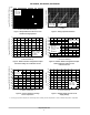
ELECTRICAL CHARACTERISTICS (V
CC
= 5.0 V, T
A
= T
low
to T
high
[Note 4], unless otherwise specified.)
Characteristics
Symbol Min Typ Max Unit
OSCILLATOR
Frequency (V
Pin
5
= 0 V, C
T
= 1.0 nF, T
A
= 25°C) f
osc
24 33 42 kHz
Charge Current (V
CC
= 5.0 V to 40 V, T
A
= 25°C) I
chg
24 35 42
mA
Discharge Current (V
CC
= 5.0 V to 40 V, T
A
= 25°C) I
dischg
140 220 260
mA
Discharge to Charge Current Ratio (Pin 7 to V
CC
, T
A
= 25°C) I
dischg
/I
chg
5.2 6.5 7.5 −
Current Limit Sense Voltage (I
chg
= I
dischg
, T
A
= 25°C) V
ipk(sense)
250 300 350 mV
OUTPUT SWITCH (Note 5)
Saturation Voltage, Darlington Connection
(I
SW
= 1.0 A, Pins 1, 8 connected)
V
CE(sat)
− 1.0 1.3 V
Saturation Voltage (Note 6)
(I
SW
= 1.0 A, R
Pin
8
= 82 W to V
CC
, Forced b ] 20)
V
CE(sat)
− 0.45 0.7 V
DC Current Gain (I
SW
= 1.0 A, V
CE
= 5.0 V, T
A
= 25°C) h
FE
50 75 − −
Collector Off−State Current (V
CE
= 40 V) I
C(off)
− 0.01 100
mA
COMPARATOR
Threshold Voltage
T
A
= 25°C
T
A
= T
low
to T
high
V
th
1.225
1.21
1.25
−
1.275
1.29
V
Threshold Voltage Line Regulation (V
CC
= 5.0 V to 40 V)
MC33063A, MC34063A
MC33063AV, NCV33063A
Reg
line
−
−
1.4
1.4
5.0
6.0
mV
Input Bias Current (V
in
= 0 V) I
IB
− −20 −400 nA
TOTAL DEVICE
Supply Current (V
CC
= 5.0 V to 40 V, C
T
= 1.0 nF, Pin 7 = V
CC
,
V
Pin
5
> V
th
, Pin 2 = GND, remaining pins open)
I
CC
− − 4.0 mA
4. T
low
= 0°C for MC34063A, −40°C for MC33063A, AV, NCV33063A
T
high
= +70°C for MC34063A, +85°C for MC33063A, +125°C for MC33063AV, NCV33063A
5. Low duty cycle pulse techniques are used during test to maintain junction temperature as close to ambient temperature as possible.
6. If the output switch is driven into hard saturation (non−Darlington configuration) at low switch currents (≤ 300 mA) and high driver currents
(≥ 30 mA), it may take up to 2.0 ms for it to come out of saturation. This condition will shorten the off time at frequencies ≥ 30 kHz, and is
magnified at high temperatures. This condition does not occur with a Darlington configuration, since the output switch cannot saturate. If a
non−Darlington configuration is used, the following output drive condition is recommended:
Forced b of output switch :
I
C
output
I
C
driver – 7.0 mA *
w 10
* The 100 W resistor in the emitter of the driver device requires about 7.0 mA before the output switch conducts.