
Datasheet


MC34063A, MC33063A, NCV33063A
http://onsemi.com
2
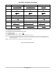
MAXIMUM RATINGS
Rating Symbol Value Unit
Power Supply Voltage V
CC
40 Vdc
Comparator Input Voltage Range V
IR
−0.3 to +40 Vdc
Switch Collector Voltage V
C(switch)
40 Vdc
Switch Emitter Voltage (V
Pin
1
= 40 V) V
E(switch)
40 Vdc
Switch Collector to Emitter Voltage V
CE(switch)
40 Vdc
Driver Collector Voltage V
C(driver)
40 Vdc
Driver Collector Current (Note 1) I
C(driver)
100 mA
Switch Current I
SW
1.5 A
Power Dissipation and Thermal Characteristics
Plastic Package, P, P1 Suffix
T
A
= 25°C P
D
1.25 W
Thermal Resistance
R
q
JA
100 °C/W
SOIC Package, D Suffix
T
A
= 25°C P
D
625 mW
Thermal Resistance
R
q
JA
160 °C/W
Operating Junction Temperature T
J
+150 °C
Operating Ambient Temperature Range T
A
°C
MC34063A 0 to +70
MC33063AV, NCV33063A −40 to +125
MC33063A −40 to +85
Storage Temperature Range T
stg
−65 to +150 °C
Maximum ratings are those values beyond which device damage can occur. Maximum ratings applied to the device are individual stress limit
values (not normal operating conditions) and are not valid simultaneously. If these limits are exceeded, device functional operation is not implied,
damage may occur and reliability may be affected.
1. Maximum package power dissipation limits must be observed.
2. This device series contains ESD protection and exceeds the following tests: Human Body Model 4000 V per MIL−STD−883, Method 3015.
Machine Model Method 400 V.
3. NCV prefix is for automotive and other applications requiring site and change control.