
Data Sheet

MC1455, MC1455B, NCV1455B
http://onsemi.com
6
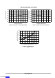
C, CAPACITANCE ( F)
μ
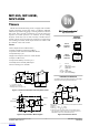
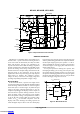
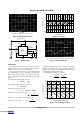
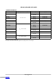
Figure 15. Monostable Waveforms Figure 16. Time Delay
Figure 17. Astable Circuit Figure 18. Astable Waveforms
(R
A
= 10 kW, C = 0.01 mF, R
L
= 1.0 kW, V
CC
= 15 V)
(R
A
= 5.1 kW, C = 0.01 mF, R
L
= 1.0 kW; R
B
= 3.9 kW, V
CC
= 15 V)
t = 20 ms/cm
t = 50 ms/cm
100
10
1.0
0.1
0.01
0.001
10 ms 100 ms
1.0 ms 10 ms 100 ms 1.0 10 100
t
d
, TIME DELAY (s)
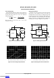
R
L
+V
CC
(5.0 V to 15 V)
Reset
V
CC
8
7Discharge
6Threshold
5
Control
Voltage
1
2
Trigger
Output
3
4
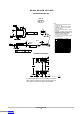
R
A
R
L
MC1455
C
R
B
Astable Mode
In the astable mode the timer is connected so that it will
retrigger itself and cause the capacitor voltage to oscillate
between 1/3 V
CC
and 2/3 V
CC
. See Figure 17.
The external capacitor changes to 2/3 V
CC
through R
A
and
R
B
and discharges to 1/3 V
CC
through R
B
. By varying the
ratio of these resistors the duty cycle can be varied. The
charge and discharge times are independent of the supply
voltage.
The charge time (output high) is given by:
t
1
+ 0.695(R
A
) R
B
)C
The discharge time (output low) is given by:
t
2
+ 0.695(R
B
)C
Thus the total period is given by:
T + t
1
) t
2
+ 0.695(R
A
) 2R
B
)C
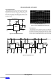
The frequency of oscillation is then:
f +
1
1
+
1.44
(R
A
) 2R
B
)C
and may be easily found as shown in Figure 19.
The duty cycle is given by:
DC +
R
B
R
A
) 2R
B
To obtain the maximum duty cycle R
A
must be as small as
possible; but it must also be large enough to limit the
discharge current (Pin 7 current) within the maximum rating
of the discharge transistor (200 mA).
The minimum value of R
A
is given by:
R
A
w
V
CC
(Vdc)
I7 (A)
w
V
CC
(Vdc)
0.2
Figure 19. Free Running Frequency
C, CAPACITANCE ( F)
μ
100
10
1.0
0.1
0.01
0.001
(R
A
+ 2 R
B
)
0.1 1.0 10 100 1.0 k 10 k 100
f, FREE RUNNING FREQUENCY (Hz)
Downloaded from Arrow.com.Downloaded from Arrow.com.Downloaded from Arrow.com.Downloaded from Arrow.com.Downloaded from Arrow.com.Downloaded from Arrow.com.