
Data Sheet
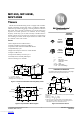

MC1455, MC1455B, NCV1455B
http://onsemi.com
2
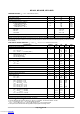
MAXIMUM RATINGS (T
A
= +25°C, unless otherwise noted.)
Rating
Symbol Value Unit
Power Supply Voltage V
CC
+18 Vdc
Discharge Current (Pin 7) I
7
200 mA
Power Dissipation (Package Limitation)
P1 Suffix, Plastic Package
Derate above T
A
= +25°C
D Suffix, Plastic Package
Derate above T
A
= +25°C
P
D
P
D
625
5.0
625
160
mW
mW/°C
mW
°C/W
Operating Temperature Range (Ambient)
MC1455B
MC1455
NCV1455B
T
A
−40 to +85
0 to +70
−40 to +125
°C
Maximum Operating Die Junction Temperature T
J
+150 °C
Storage Temperature Range T
stg
−65 to +150 °C
Stresses exceeding Maximum Ratings may damage the device. Maximum Ratings are stress ratings only. Functional operation above the
Recommended Operating Conditions is not implied. Extended exposure to stresses above the Recommended Operating Conditions may affect
device reliability.
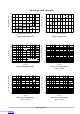
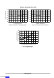
ELECTRICAL CHARACTERISTICS (T
A
= +25°C, V
CC
= +5.0 V to +15 V, unless otherwise noted.)
Characteristics
Symbol Min Typ Max Unit
Operating Supply Voltage Range V
CC
4.5 − 16 V
Supply Current
V
CC
= 5.0 V, R
L
= R
V
CC
= 15 V, R
L
= R, Low State (Note 1)
I
CC
−
−
3.0
10
6.0
15
mA
Timing Error (R = 1.0 kW to 100 kW) (Note 2)
Initial Accuracy C = 0.1 mF
Drift with Temperature
Drift with Supply Voltage
−
−
−
1.0
50
0.1
−
−
−
%
PPM/°C
%/V
Threshold Voltage/Supply Voltage V
th
/V
CC
− 2/3 −
Trigger Voltage
V
CC
= 15 V
V
CC
= 5.0 V
V
T
−
−
5.0
1.67
−
−
V
Trigger Current I
T
− 0.5 −
mA
Reset Voltage V
R
0.4 0.7 1.0 V
Reset Current I
R
− 0.1 − mA
Threshold Current (Note 3) I
th
− 0.1 0.25
mA
Discharge Leakage Current (Pin 7) I
dischg
− − 100 nA
Control Voltage Level
V
CC
= 15 V
V
CC
= 5.0 V
V
CL
9.0
2.6
10
3.33
11
4.0
V
Output Voltage Low
I
Sink
= 10 mA (V
CC
= 15 V)
I
Sink
= 50 mA (V
CC
= 15 V)
I
Sink
= 100 mA (V
CC
= 15 V)
I
Sink
= 200 mA (V
CC
= 15 V)
I
Sink
= 8.0 mA (V
CC
= 5.0 V)
I
Sink
= 5.0 mA (V
CC
= 5.0 V)
V
OL
−
−
−
−
−
−
0.1
0.4
2.0
2.5
−
0.25
0.25
0.75
2.5
−
−
0.35
V
Output Voltage High
V
CC
= 15 V (I
Source
= 200 mA)
V
CC
= 15 V (I
Source
= 100 mA)
V
CC
= 5.0 V (I
Source
= 100 mA)
V
OH
−
12.75
2.75
12.5
13.3
3.3
−
−
−
V
Rise Time Differential Output t
r
− 100 − ns
Fall Time Differential Output t
f
− 100 − ns
1. ‘Supply current when output is high is typically 1.0 mA less.
2. Tested at V
CC
= 5.0 V and V
CC
= 15 V Monostable mode.
3. This will determine the maximum value of R
A
+ R
B
for 15 V operation. The maximum total R = 20 MW .
4. T
low
= 0°C for MC1455, T
low
= −40°C for MC1455B, NCV1455B
T
high
= +70°C for MC1455, T
high
= +85°C for MC1455B, T
high
= +125°C for NCV1455B
5. NCV prefix is for Automotive and other applications requiring site and change control.
Downloaded from Arrow.com.Downloaded from Arrow.com.