
Datasheet
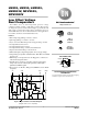


LM393, LM293, LM2903, LM2903V, NCV2903, NCV2903V
http://onsemi.com
3
ELECTRICAL CHARACTERISTICS (V
CC
= 5.0 Vdc, T
low
≤ T
A
≤ T
high
, unless otherwise noted.)
Characteristic
Symbo
l
LM293, LM393
LM2903, LM2903V,
NCV2903, NCV2903V
Unit
Min Typ Max Min Typ Max
Input Offset Voltage (Note 6) V
IO
mV
T
A
= 25°C − ±1.0 ±5.0 − ±2.0 ±7.0
T
low
≤ T
A
≤ T
high
− − ±9.0 − ±9.0 ±15
Input Offset Current I
IO
nA
T
A
= 25°C − ±5.0 ±50 − ±5.0 ±50
T
low
≤ T
A
≤ T
high
− − ±150 − ±50 ±200
Input Bias Current (Note 7) I
IB
nA
T
A
= 25°C − 20 250 − 20 250
T
low
≤ T
A
≤ T
high
− − 400 − 20 500
Input Common Mode Voltage Range (Note 7) V
ICR
V
T
A
= 25°C 0 − V
CC
−1.5 0 − V
CC
−1.5
T
low
≤ T
A
≤ T
high
0 − V
CC
−2.0 0 − V
CC
−2.0
Voltage Gain A
VOL
50 200 − 25 200 − V/mV
R
L
≥ 15 k, V
CC
= 15 Vdc, T
A
= 25°C
Large Signal Response Time − − 300 − − 300 − ns
V
in
= TTL Logic Swing, V
ref
= 1.4 Vdc
V
RL
= 5.0 Vdc, R
L
= 5.1 k, T
A
= 25°C
Response Time (Note 9) t
TLH
− 1.3 − − 1.5 −
s
V
RL
= 5.0 Vdc, R
L
= 5.1 k, T
A
= 25°C
Input Differential Voltage (Note 10) V
ID
− − V
CC
− − V
CC
V
All V
in
≥ GND or V− Supply (if used)
Output Sink Current I
Sink
6.0 16 − 6.0 16 − mA
V
in
≥ 1.0 Vdc, V
in+
= 0 Vdc, V
O
≤ 1.5 Vdc T
A
= 25°C
Output Saturation Voltage V
OL
mV
V
in
≥ 1.0 Vdc, V
in+
= 0, I
Sink
≤ 4.0 mA, T
A
= 25°C − 150 400 − − 400
T
low
≤ T
A
≤ T
high
− − 700 − 200 700
Output Leakage Current I
OL
nA
V
in−
= 0 V, V
in+
≥ 1.0 Vdc, V
O
= 5.0 Vdc, T
A
= 25°C − 0.1 − − 0.1 −
V
in−
= 0 V, V
in+
≥ 1.0 Vdc, V
O
= 30 Vdc,
T
low
≤ T
A
≤ T
high
− − 1000 − − 1000
Supply Current I
CC
mA
R
L
= ∞ Both Comparators, T
A
= 25°C − 0.4 1.0 − 0.4 1.0
R
L
= ∞ Both Comparators, V
CC
= 30 V − − 2.5 − − 2.5
Product parametric performance is indicated in the Electrical Characteristics for the listed test conditions, unless otherwise noted. Product
performance may not be indicated by the Electrical Characteristics if operated under different conditions.
LM293 T
low
= −25°C, T
high
= +85°C
LM393 T
low
= 0°C, T
high
= +70°C
LM2903 T
low
= −40°C, T
high
= +105°C
LM2903V & NCV2903 T
low
= −40°C, T
high
= +125°C
NCV2903V T
low
= −40°C, T
high
= +150°C
NCV2903 and NCV2903V are qualified for automotive use.
5. The maximum output current may be as high as 20 mA, independent of the magnitude of V
CC
, output short circuits to V
CC
can cause
excessive heating and eventual destruction.
6. At output switch point, V
O
]1.4 Vdc, R
S
= 0 with V
CC
from 5.0 Vdc to 30 Vdc, and over the full input common mode range
(0 V to V
CC
= −1.5 V).
7. Due to the PNP transistor inputs, bias current will flow out of the inputs. This current is essentially constant, independent of the output state,
therefore, no loading changes will exist on the input lines.
8. Input common mode of either input should not be permitted to go more than 0.3 V negative of ground or minus supply. The upper limit of
common mode range is V
CC
−1.5 V.
9. Response time is specified with a 100 mV step and 5.0 mV of overdrive. With larger magnitudes of overdrive faster response times are
obtainable.
10.The comparator will exhibit proper output state if one of the inputs becomes greater than V
CC
, the other input must remain within the common
mode range. The low input state must not be less than −0.3 V of ground or minus supply.