
Datasheet


LM358, LM258, LM2904, LM2904V
3
MOTOROLA ANALOG IC DEVICE DATA
Single Supply Split Supplies
V
CC
V
EE
/Gnd
3.0 V to V
CC(max)
1
2
V
CC
1
2
V
EE
1.5 V to V
CC(max)
1.5 V to V
EE(max)
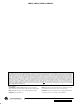
Representative Schematic Diagram
(One–Half of Circuit Shown)
Output
Bias Circuitry
Common to Both
Amplifiers
V
CC
V
EE
/Gnd
Inputs
Q2
Q3 Q4
Q5
Q26
Q7
Q8
Q6
Q9
Q11
Q10
Q1
2.4 k
Q25
Q22
40 k
Q13
Q14
Q15
Q16
Q19
5.0 pF
Q18
Q17
Q20
Q21
2.0 k
Q24
Q23
Q12
25
CIRCUIT DESCRIPTION
The LM258 series is made using two internally
compensated, two–stage operational amplifiers. The first
stage of each consists of differential input devices Q20 and
Q18 with input buffer transistors Q21 and Q17 and the
differential to single ended converter Q3 and Q4. The first
stage performs not only the first stage gain function but also
performs the level shifting and transconductance reduction
functions. By reducing the transconductance, a smaller
compensation capacitor (only 5.0 pF) can be employed, thus
saving chip area. The transconductance reduction is
accomplished by splitting the collectors of Q20 and Q18.
Another feature of this input stage is that the input common
mode range can include the negative supply or ground, in
single supply operation, without saturating either the input
devices or the differential to single–ended converter. The
second stage consists of a standard current source load
amplifier stage.
Each amplifier is biased from an internal–voltage regulator
which has a low temperature coefficient thus giving each
amplifier good temperature characteristics as well as
excellent power supply rejection.
Large Signal Voltage
Follower Response
5.0
µ
s/DIV
1.0 V/DIV
V
CC
= 15 Vdc
R
L
= 2.0 k
Ω
T
A
= 25
°
C