
Data Sheet


KA78RH33R — Low Dropout Voltage Regulator
© 2001 Fairchild Semiconductor Corporation www.fairchildsemi.com
KA78RH33R Rev. 1.1.0 2
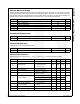
Absolute Maximum Ratings
Stresses exceeding the absolute maximum ratings may damage the device. The device may not function or be opera-
ble above the recommended operating conditions and stressing the parts to these levels is not recommended. In addi-
tion, extended exposure to stresses above the recommended operating conditions may affect device reliability. The
absolute maximum ratings are stress ratings only. Values are at T
A
= 25°C unless otherwise noted.
Temperature Characteristics
Thermal Characteristics
Values are at T
A
= 25°C unless otherwise noted.
Electrical Characteristics
Refer to the test circuit, values are at V
IN
= 5 V, C
O
= 10 μF, and T
A
= 25°C,unless otherwise specified.
Symbol Parameter Value Unit
V
IN
Power Supply Input Voltage 15 V
I
O
Output Load Current 800 mA
T
J
Junction Temperature 150 °C
T
OPR
Operating Junction Temperature -25 to 125 °C
T
STG
Storage Temperature -55 to 150 °C
Symbol Parameter Value Unit
ΔV
O
/ ΔT Temperature Coefficient of Output Voltage ±0.02 %/ °C
Symbol Parameter Value Unit
R
θJA
Thermal Resistance, Junction to Ambient 110 °C/W
Symbol Parameter Conditions Min. Typ. Max. Unit
V
OUT
Output Voltage I
O
= 10 mA, T
J
= 25°C 3.27 3.30 3.33 V
V
OUT
Output Voltage
V
IN
= 4.8 V to 12 V,
I
O
= 10 mA to 800 mA,
T
J
= -25°C to 125°C
3.23 3.30 3.37 V
R
line
Line Regulation V
IN
= 4.8 V to 12 V, I
O
= 10 mA 1 10 mV
R
load
Load Regulation I
O
= 10 mA to 800 mA 1 20 mV
RR Ripple Rejection
f = 120 Hz, I
O
= 500 mA,
V
IN
= 6.3 ± 1 Vrms
55 dB
V
drop
Dropout Voltage
I
O
= 100 mA 1.00 1.20
VI
O
= 500 mA 1.05 1.25
I
O
= 800 mA 1.10 1.40
I
q
Quiescent Current V
IN
≤ 12 V 5 10 mA
ΔV
O
/ ΔT
Temperature Coefficient
of Output Voltage
T
J
= -25°C to 125°C,
I
O
= 10 mA
0.2 mV/°C
I
pk
Peak Output Current V
IN
= 6.3 V 800 mA
V
n
Output Noise Voltage f = 10 Hz to 10 kHz 100 μVrms