
Data Sheet


© 2003 Fairchild Semiconductor Corporation www.fairchildsemi.com
KA7500C • Rev. 1.0.2 4
KA7500C — SMPS Controller
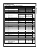
Absolute Maximum Ratings
Stresses exceeding the absolute maximum ratings may damage the device. The device may not function or be
operable above the recommended operating conditions and stressing the parts to these levels is not recommended.
In addition, extended exposure to stresses above the recommended operating conditions may affect device
reliability. The absolute maximum ratings are stress ratings only.
Symbol Parameter Min. Max. Unit
V
CC
Supply Voltage 42 V
V
C
Collector Supply Voltage 42 V
I
O
Output Current 250 mA
V
IN
Amplifier Input Voltage V
CC
+ 0.3 V
KA7500C 1
P
D
Power Dissipation
KA7500CD 0.9
W
T
OPR
Operation Temperature Range -25 +85 °C
T
STG
Storage Temperature Rang -65 +150 °C
T
J
Junction Temperature +125 °C
Recommended Operating Conditions
The Recommended Operating Conditions table defines the conditions for actual device operation. Recommended
operating conditions are specified to ensure optimal performance to the datasheet specifications. Fairchild does not
recommend exceeding them or designing to Absolute Maximum Ratings.
Symbol Parameter Min. Typ. Max. Unit
V
CC
Power Supply Voltage 7 15 40 V
V
C1
, V
C2
Collector Supply Voltage 30 40 V
I
C1
, I
C2
Collector Output Current (Each Transition) 200 mA
V
IN
Amplifier Input Voltage 0.3 V
CC
- 2.0 V
I
FB
Current Into Feedback Terminal 0.3 mA
I
REF
Reference Output Terminal 10 mA
R
T
Timing Resistor 1.8 30.0 500.0
KΩ
C
T
Timing Capacitor 0.0047 0.0010 10.0000 µA
f
OSC
Oscillator Frequency 1 40 200 kHz
V
IN_PWM
PWM Input Voltage (Pins 3, 4, and 13) 0.3 5.3 V