
Data Sheet


KA5L0380R S P S
Preliminary
TYPICAL PERFORMANCE CHARACTERISTICS (Continued)
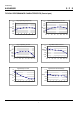
- 50 0 50 100 150
0.8
0.9
1.0
1.1
1.2
@ Notes :
1. V
GS
= 0V
2. I
D
= 250
µ
A
T
J
, Junction Temperature [
o
C]
BV
DSS
, (Normalized)
Drain-Source Breakdown Voltage
- 50 0 50 100 150
0.0
0.5
1.0
1.5
2.0
2.5
R
DS(on)
, (Normalized)
Drain-Source On-Resistance
T
J
, Junction Temperature [
o
C]
@ Notes:
1. V
GS
= 10V
2. I
D
= 1.5 A
10
1
10
2
10
3
10
-2
10
-1
10
0
10
1
10
2
100
µ
s
DC
10
µ
s
1 ms
10 ms
@ Notes :
1. T
C
= 25
o
C
2. T
J
= 150
o
C
3. Single Pulse
Operation in This Area
is Limited by R
DS(on)
I
D
, Drain Current [A]
V
DS
, Drain-Source Voltage [V]
40 60 80 100 120 140
0.0
0.5
1.0
1.5
2.0
2.5
3.0
3.5
I
D
, Drain Current [A]
T
C
, Case Temperature [
o
C]
10
-5
10
-4
10
-3
10
-2
10
-1
10
0
10
1
10
-2
10
-1
10
0
single pulse
0.2
0.1
0.01
0.02
0.05
D=0.5
@ Notes :
1. Z
θ
JC
(t)=1.25
o
C/W Max.
2. Duty Factor, D=t
1
/t
2
3. T
JM
-T
C
=P
DM
*Z
θ
JC
(t)
Z
θ
JC
(t) , Thermal Response
t
1
, Square Wave Pulse Duration [sec]
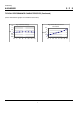
Fig. 8 On-Resistance vs. Temperature Fig. 7 Breakdown Voltage vs. Temperature
Fig. 10 Max. Drain Current vs. Case Temperature Fig. 9 Max. Safe Operating Area
Fig. 11 Thermal Response
www.onsemi.com
6